Hangzhou Tuya Inc.
NM1 Module Hardware Design Manual
https://www.tuya.com
Page 17 of 29
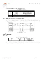
3.5 SPIs
3.5.1 Pins
Table 3-7 defines the SPI signals. (SPIs support the slave mode.)
Table 3- 5 SPI signal definition
Pin No.
Signal Name
Function Description
3
SPI_MISO
Master input and slave output
4
SPI_MOSI
Master output and slave input
5
SPI_ SCLK
SPI clock signal
6
SPI_CS
SPI selection signal
3.5.2 SPI Electrical Parameters and Application
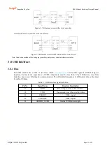
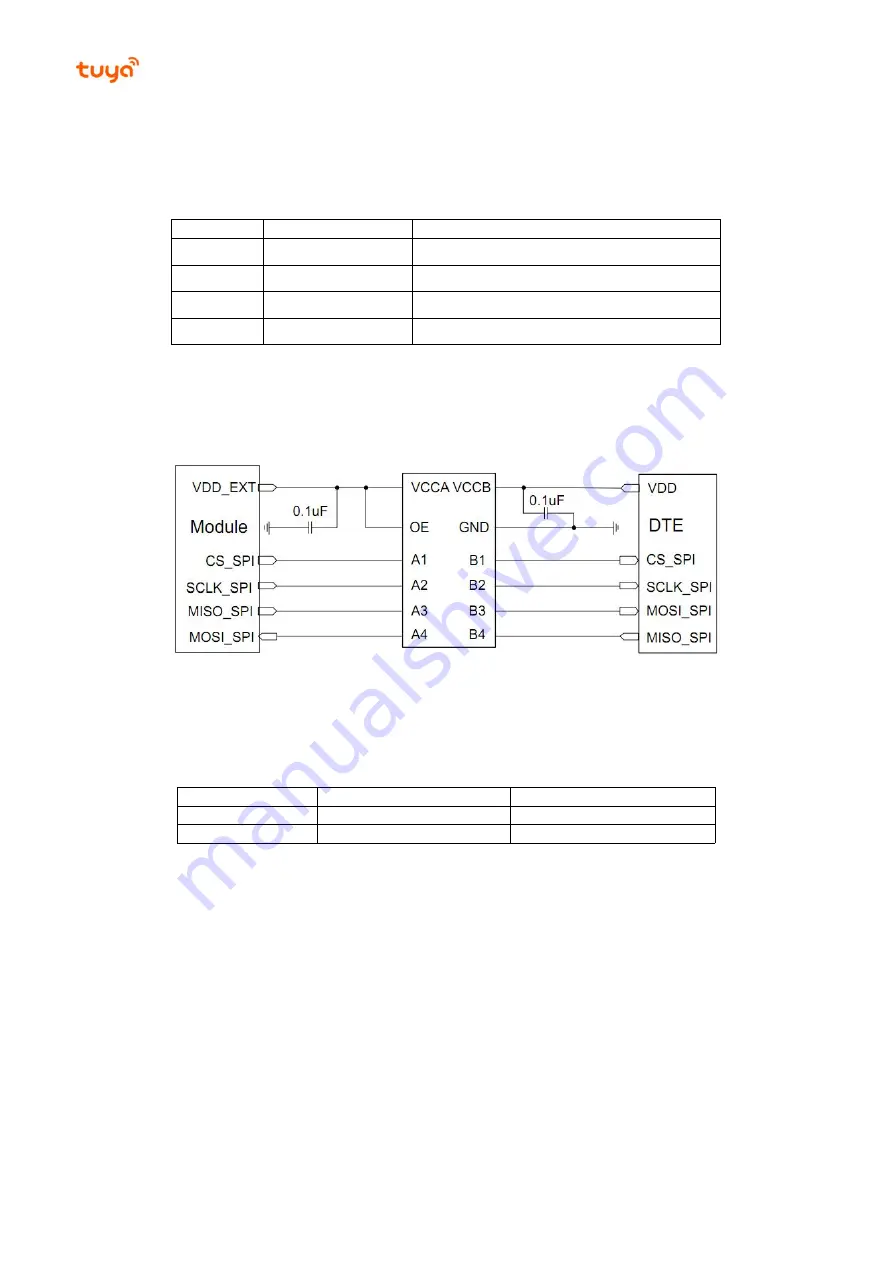
The level of the SPI on the NM1 module is 1.8 V. If the host level is 3.3 V, add a level converter between the
NM1 module and host. The level converter that supports the SPI data rate is recommended. Figure 3- 4 shows
the reference circuit.
Figure 3- 4 Reference circuit
3.6 I
2
C Interface
3.6.1 Pins
Table 3- 6 I
2
C interface signal definition
Pin No.
Signal Name
Function Description
32
SDA
I
2
C serial data
33
SCL
I
2
C serial clock
I
2
C is a two-line bus for communication between ICs. It has a serial data cable (SDA) and a serial clock cable
(SCL) to transmit information between connected devices. I
2
C identifies each device based on its unique
address and can be used as both a transmitter and a receiver.


