background image

7 POWER-ON SEQUENCE AND RESETTING

7 Power-on Sequence and Resetting

7.1 Power-on Sequence

The RTL8720CF chip has requirements on the power-on sequence.

It is recom-

mended that the voltage rise from 0 to 3.3V within 40mS.

Symbol

Parameter

Minimum

Value

Typical
Value

Maximum

Value

Unit

TPRDY

3.3V ready
time

0.6

20

mS

CHIP_EN

CHIP_EN
ready time

0.6

20

mS

7.2 Resetting

When designing a plate of a module, you should set a reset IC at the foot of CHIP_EN

in advance. The preferable type of IC is BL8506-27CRO. The module is packaged in
the form of SOT23. For solutions to starting a module in some cases, refer to the
circuit in the following figure (R30 is preset and cannot be placed).

13 / 25

Summary of Contents for WBR3L

Page 1: ...WBR3L Module Datasheet Device Development Cloud Module WiFi BT Dual Mode Module Version 20200812 Online Version ...

Page 2: ...ng Power Consumption 8 5 RF Parameters 9 5 1 Basic RF Features 9 5 2 TX Performance 9 5 3 RX Performance 11 6 Antenna Information 12 6 1 Antenna Type 12 6 2 Antenna Interference Reduction 12 7 Power on Sequence and Resetting 13 7 1 Power on Sequence 13 7 2 Resetting 13 8 Packaging Information and Production Instructions 15 8 1 Mechanical Dimensions 15 8 2 Recommended PCB Layout 16 8 3 Pin Header S...

Page 3: ...Contents 8 6 Storage Conditions 22 9 MOQ and Packaging Information 23 10 Appendix Statement 23 ii ...

Page 4: ...d WiFi products as required 1 1 Features 1 Embedded low power KM4 MCU which can also function as an application pro cessor Clock rate 100MHz 2 Working voltage 3 0 to 3 6 V 3 Peripherals 9 GPIOs 1 universal asynchronous receiver transmitter UART and 1 log transmitter 4 WiFi BT connectivity 802 11 B G N20 Channels 1 to 14 at 2 4 Ghz channels 1 to 11 for US CA and channels 1 to 13 for EU CN Support W...

Page 5: ...1 PRODUCT OVERVIEW Baby monitor Network camera Intelligent bus 2 25 ...

Page 6: ...n after Update 1 3 21 2020 This is the first release V1 0 0 3 Module Interfaces 3 1 Dimensions and Footprint WBR3L has two rows of pins with a 2 mm pin spacing Each row has 8 pins The WBR3L dimensions are 16 0 35 mm W 24 0 35 mm L 2 9 0 15 mm H The dimensions of WBR3L are as follows 3 25 ...

Page 7: ...odules 2 A_7 I O GPIOA_7 hardware PWM IC Pin 21 3 EN I O Enabling pin which works at the high level and is pulled up and controlled by a user externally 4 A_11 I O GPIOA_11 hardware PWM IC Pin 25 5 A_2 I O GPIOA_2 hardware PWM IC Pin 18 6 A_3 I O GPIOA_3 hardware PWM IC Pin 19 7 A_4 I O GPIOA_4 hardware PWM IC Pin 20 8 VCC P Power supply pin 3 3V 9 GND P Power supply reference ground 4 25 ...

Page 8: ...can be configured as a common GPIO 12 A_17 I O GPIOA_17 hardware PWM IC Pin 38 13 A_18 I O GPIOA_18 hardware PWM IC Pin 39 14 A_19 I O GPIOA_19 hardware PWM IC Pin 40 15 RXD I O GPIOA_13 UART0_RXD which is used as a user side serial interface pin 16 TXD I O GPIOA_14 UART0_TXD which is used as a user side serial interface pin Note P indicates power supply pins and I O indicates input output pins 5 2...

Page 9: ...ge temperature 40 125 VDD Power supply voltage 0 3 3 6 V Static electricity discharge voltage human body model TAMB 25 2 KV Static electricity discharge voltage machine model TAMB 25 0 5 KV 4 2 Working Conditions Parameter Description Minimum Value Typical Value Maximum Value Unit Ta Working tempera ture 20 105 VDD Working voltage 3 0 3 6 V 6 25 ...

Page 10: ...el input 2 0 V VOL I O low level output 0 4 V VOH I O high level output 2 4 V Imax I O drive current 16 mA Cpad Input pin capaci tance 2 pF 4 3 RF Power Consumption 1 TX power consumption Symbol Mode Average Value Peak Value Typical Value Unit IRF 11B 11M 63 65 mA IRF 11G 54M 65 67 mA IRF 11N HT20 MCS7 65 67 mA 2 RX power consumption 7 25 ...

Page 11: ... Average Value Peak Value Typical Value Unit Quick connection network status The module is in the fast network connection state and the WiFi indicator always flashes 75 324 mA Network connection idle state The module is connected to the network and the WiFi indicator is always on 64 314 mA Network connection operation status The module is connected to the network and the WiFi indicator is always on...

Page 12: ... Parameters 5 1 Basic RF Features Parameter Description Frequency range 2 400 to 2 4835 GHz WiFi standard IEEE 802 11b g n channels 1 to 14 BLE standard Bluetooth 4 2 Data transmission rate Data transmission rate Data transmission rate 11g 6 9 12 18 24 36 48 54 Mbps Data transmission rate 11n HT20 MCS 0 to 7 Antenna Type PCB antenna with a gain of 1 82 dBi 5 2 TX Performance 9 25 ...

Page 13: ...CK Mode 1 Mbit s 17 5 dBm Average RF output power 802 11g OFDM mode 54 Mbit s 14 5 dBm Average RF output power 802 11n OFDM mode MCS7 13 5 dBm Average RF output power BLE 4 2 1 Mbit s 6 5 dBm Frequency error 20 20 ppm EVM 802 11b CCK 11Mbps Mode 17 5dBm 10 dB EVM 802 11g OFDM 54Mbps Mode 14 5dBm 29 dB 10 25 ...

Page 14: ...S7 Mode 13 5dBm 30 dB 5 3 RX Performance Parameter Minimum Value Typical Value Maximum Value Unit PER 8 RX sensitivity 802 11b CCK Mode 1M 91 dBm PER 10 RX sensitivity 802 11g OFDM Mode 54M 75 dBm PER 10 RX sensitivity 802 11n OFDM Mode MCS7 72 dBm PER 10 RX sensitivity BLE 4 2 1M 93 dBm 11 25 ...

Page 15: ...3L uses only an onboard PCB antenna with a gain of 1 82 dBi 6 2 Antenna Interference Reduction To ensure optimal WiFi performance when the WiFi module uses an onboard PCB antenna it is recommended that the antenna be at least 15 mm away from other metal parts 12 25 ...

Page 16: ...imum Value Typical Value Maximum Value Unit TPRDY 3 3V ready time 0 6 20 mS CHIP_EN CHIP_EN ready time 0 6 20 mS 7 2 Resetting When designing a plate of a module you should set a reset IC at the foot of CHIP_EN in advance The preferable type of IC is BL8506 27CRO The module is packaged in the form of SOT23 For solutions to starting a module in some cases refer to the circuit in the following figure...

Page 17: ...7 POWER ON SEQUENCE AND RESETTING 14 25 ...

Page 18: ... INSTRUCTIONS 8 Packaging Information and Production Instructions 8 1 Mechanical Dimensions The mechanical dimensions of PCB of WBR3L are 16 0 35 mm W 24 0 35 mm L 0 8 0 1 mm H The following figure shows mechanical dimensions of WBR3L 15 25 ...

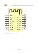
Page 19: ...lt dimensional tolerance is 0 35 mm If you have specific require ments on dimensions make them clear in the datasheet after communication 8 2 Recommended PCB Layout The following figure is a schematic diagram of WBR3L which shows how pins corre spond to each other 16 25 ...

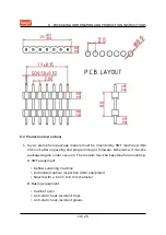
Page 20: ...8 PACKAGING INFORMATION AND PRODUCTION INSTRUCTIONS WBR3L PCB Layout is shown as belows 17 25 ...

Page 21: ...INSTRUCTIONS 8 3 Pin Header Specifications WBR3L has two models WBR3L with pin headers and WBR3L without pin headers Which one is used depends on actual situations Dimensions and recommended layout of pin headers are as follows unit mm 18 25 ...

Page 22: ...urs after unpacking and programming of firmware Otherwise it must be packaged again under vacuum The module must be baked before mounting A SMT equipment Reflow soldering machine Automated optical inspection AOI equipment Nozzle with a 6 mm to 8 mm diameter B Baking equipment Cabinet oven Anti static heat resistant trays Anti static heat resistant gloves 19 25 ...

Page 23: ...ke the module for 6 consecutive hours If the 30 40 and 50 circles are pink bake the module for 12 consecutive hours 4 Baking settings Baking temperature 125 5 C Alarm temperature 130 C SMT ready temperature after natural cooling 36 C The number of drying times 1 Rebaking condition The module is not soldered within 12 hours after baking 5 Do not use SMT to process modules that have been unpacked fo...

Page 24: ...s from subsequent batches each hour for visual inspection and AOI 8 5 Recommended Oven Temperature Curve Perform SMT based on the following reflow oven temperature curve The highest temperature is 245 C The reflow temperature curve is shown as belows Refer to IPC JEDEC standard Peak Temperature 245 The number of Times 2 times 21 25 ...

Page 25: ...8 PACKAGING INFORMATION AND PRODUCTION INSTRUCTIONS 8 6 Storage Conditions 22 25 ...

Page 26: ...a residential installation This equipment generates uses and can radiate radio frequency energy and if not installed and used in accordance with the instructions may cause harmful interference to radio communications However there is no guarantee that interference will not occur in a particular installation If this equipment does cause harmful interference to radio or television reception which ca...

Page 27: ...n in this manual including This product must be installed and operated with a mini mum distance of 20 cm between the radiator and user body This device have got a FCC ID 2ANDL WBR3L The final end product must be labeled in a visible area with the following Contains Transmitter Module FCC ID 2ANDL WBR3L This device is intended only for OEM integrators under the following conditions 1 The antenna mus...

Page 28: ...sposed of as normal household waste in accordance with EU directive for waste electrical and electronic equipment WEEE 2012 19 EU Instead it should be disposed of by returning it to the point of sale or to a municipal recycling collection point 25 25 ...

Reviews: