


AMY-5M
-
Hardware
Integration
Manual
Objective
Specification
Design-In
GPS.G5-MS5-08207
u-blox
proprietary
Page 18
your position is our focus
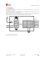
2.2 System Functions
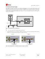
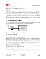
2.2.1 EXTINT - External Interrupt Pin
EXTINT0
is
an
external
interrupt
pin.
It
will
be
used
in
future
AMY-5M
releases
for
wake-up
functions
in
low-
power
modes.
2.2.2 System
Monitoring
The
u-blox
-
5
GPS
Receiver
provides
System
Monitoring
functions
that
allow
the
operation
of
the
embedded
processor
and
associated
peripherals
to
be
supervised.
These
System
Monitoring
functions
are
being
output
as
part
of
the
UBX
protocol,
class
‘MON’.
Please
refer
to
the
u-blox 5
Protocol Specification
[3].
For
more
information
on
UBX
messages,
serial
interfaces
for
design
analysis
and
individual
system
monitoring
functions.
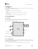
2.3 Interfaces
2.3.1 Serial
UART
1
(
RxD1
/
TxD1
)
is
the
default
serial
interface.
It
supports
data
rates
from
4.8
kBit/s
to
115
kBit/s.
An
interface
based
on
RS232
standard
levels
(+/-
12
V)
can
be
realized
using
level
shifters
such
as
Maxim
MAX3232.
The
TxD1
output
levels
are
dependant
on
VDD_IO.
(see
AMY-5M Data Sheet
[2]).
The
RxD1
has
fixed
input
voltage
thresholds,
which
do
not
depend
on
VDD_IO
(see
AMY-5M Data Sheet
[2]).
For
the
default
settings
see
the
AMY-5M Data Sheet
[2].
Hardware
handshake
signals
and
synchronous
operation
are
not
supported.
2.3.2 USB
The
u-blox
5
USB
interface
supports
the
full-speed
data
rate
of
12
Mbit/s.
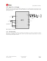
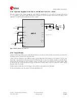
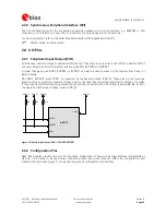
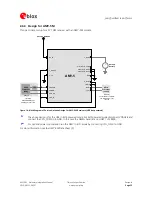
2.3.2.1
USB external components
The
USB
interface
requires
some
external
components
in
order
to
implement
the
physical
characteristics
required
by
the
USB
2.0
specification.
These
external
components
are
shown
in
Figure
9
and
listed
in
Table
4.
In
order
to
comply
with
USB
specifications,
VBUS
must
be
connected
through
an
LDO
(U1)
to
pin
VDD_USB
of
the
module.
If
the
USB
device
is
self-powered
it
is
possible
that
the
power
supply
(V_DCDC)
is
shut
down
and
the
Baseband-IC
core
is
not
powered.
Since
VBUS
is
still
available,
it
still
would
be
signaled
to
the
USB
host
that
the
device
is
present
and
ready
to
communicate.
This
is
not
desired
and
thus
the
LDO
(U1)
should
be
disabled
using
the
enable
signal
(EN)
of
the
VDD_USB-LDO
or
the
output
of
a
voltage
supervisor.
Depending
on
the
characteristics
of
the
LDO
(U1)
it
is
recommended
to
add
a
pull-down
resistor
(R11)
at
its
output
to
ensure
VDD_USB
is
not
floating
if
LDO
(U1)
is
disabled
or
the
USB
cable
is
not
connected
i.e.
VBUS
is
not
supplied.
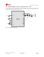
If
the
device
is
bus-powered
,
LDO
(U1)
does
not
need
an
enable
control.
All
u-blox
5
receivers
based
on
ROM
5.00
and
above
support
both
Bus
and
Self
Powered
Mode
on
the
USB
interface.
Please
be
sure
to
use
the
latest
drivers
from
our
website.
Connect
VDD_USB
to
GND
if
not
used.