AMY-5M
-
Hardware
Integration
Manual
Objective
Specification
Design-In
GPS.G5-MS5-08207
u-blox
proprietary
Page 27
your position is our focus
Standard Function
Remarks
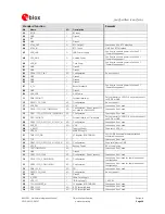
No
Name
I/O
Description
G5
PIO5
/
TxD1
I/O
Asynchronous
Serial
Leave
open
if
not
used.
G6
PIO4
/
RxD1
I
Asynchronous
Serial
Pull-up
resistor
to
VDDIO.
If
not
used
connect
to
VDDB
or
GND.
G7
V_BCKP
I
Backup
voltage
supply
1.4-3.6V
(optional).
Connect
to
GND
if
not
used
G8
VDD_C
O
Core
Power
NC
or
supply
cap
G9
NC
O
Not
Connected
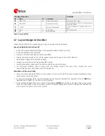
Table 5: Pinout AMY-5M
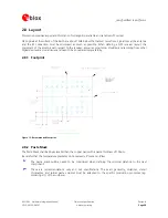
2.7 Layout Design-In Checklist
Follow
this
checklist
for
the
Layout
design
to
get
an
optimal
GPS
performance.
Layout optimizations (
Section 2.8
)
Is
the
GPS
module
placed
according
to
the
recommendation
in
Section 2.8.3
?
Is
the
Grounding
concept
optimal?
Has
the
micro
strip
been
kept
as
short
as
possible?
Assure
low
serial
resistance
in
V_DCDC
power
supply
line
(choose
a
line
width
>400um)
Keep
power
supply
line
as
short
as
possible
Design
a
guard
ring
around
the
optional
RTC
crystal
Add
a
ground
plane
underneath
the
GPS
module
to
reduce
interference.
For
improved
shielding,
add
as
many
vias
as
possible
around
the
micro
strip,
around
the
serial
communication
lines,
underneath
the
GPS
module
etc.
Calculation of the micro strip
The
micro
strip
must
be
50
Ohms
and
be
routed
in
a
section
of
the
PCB
where
minimal
interference
from
noise
sources
can
be
expected.
In
case
of
a
multi-layer
PCB,
use
the
thickness
of
the
dielectric
between
the
signal
and
the
1st
GND
layer
(typically
the
2nd
layer)
for
the
micro
strip
calculation.
If
the
distance
between
the
micro
strip
and
the
adjacent
GND
area
(on
the
same
layer)
does
not
exceed
5
times
the
track
width
of
the
micro
strip,
use
the
“Coplanar
Waveguide”
model
in
AppCad
to
calculate
the
micro
strip
and
not
the
“micro
strip”
model.

