background image


AMY-5M


-


Hardware


Integration


Manual


Objective


Specification


Design-In


GPS.G5-MS5-08207


u-blox


proprietary


Page 28


 your position is our focus

2.8  Layout  

This


section


provides


important


information


for


designing


a


reliable


and


sensitive


GPS


system.


GPS


signals


at


the


surface


of


the


Earth


are


about


15dB


below


the


thermal


noise


floor.


Signal


loss


at


the


antenna


and


the


RF


connection


must


be


minimized


as


much


as


possible.


When


defining


a


GPS


receiver


layout,


the


placement


of


the


antenna


with


respect


to


the


receiver,


as


well


as


grounding,


shielding


and


jamming


from


other


digital


devices


are


crucial


issues


and


need


to


be


considered


very


carefully.


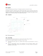
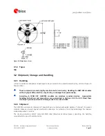
2.8.1 Footprint 


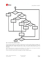
Figure 15: Recommended footprint 

2.8.2 Paste 

Mask 

The


Paste


Mask


shall


be


50

μ

m


smaller


than


the


copper


pads


with


a


paste


thickness


of


100

μ

m.


Be


careful


that


the


temperature


gradients


do


not


exceed


+2º/sec


and


-4º/sec.


The


paste


mask


outline


needs


to


be


considered


when


defining


the


minimal


distance


to


the


next


component.


These


are


recommendations


only


and


not


specifications.


The


exact


geometry,


distances,


stencil


thicknesses


and


solder


paste


volumes


must


be


adapted


to


the


specific


production


processes


(e.g.


soldering


etc.)


of


the


customer.


Summary of Contents for AMY-5M

Page 1: ...s smallest form factor and is a fully tested standalone solution that requires no additional components and no host integration This module combines exceptional GPS performance with highly flexible po...

Page 2: ...isclosure to third parties without express permission is strictly prohibited Copyright 2008 u blox AG u blox is a registered trademark of u blox Holding AG in the EU and other countries ARM is the reg...

Page 3: ...eginning to the end To help in finding needed information a brief section overview is provided below 1 Hardware Basics This chapter introduces the basics of function and architecture of the AMY 5 modu...

Page 4: ...er than any personal email address of our staff This makes sure that your request is processed as soon as possible You will find the contact details at the end of the document Helpful Information when...

Page 5: ...5 Single 2 5 3 6 V Supply 13 2 1 6 Single 1 75 2 0 V Supply 14 2 1 7 Separate Supplies of 1 8 V 1 75 2 0V and 1 4 V 1 4 3 6 V 15 2 1 8 Separate Supplies of 3 0 V 2 5 3 6 0V and 1 4 V 1 4 3 6 V 16 2 1...

Page 6: ...cautions for Antennas 30 3 Product Handling 31 3 1 Packaging 31 3 1 1 Reels 31 3 1 2 Tapes 32 3 2 Shipment Storage and Handling 32 3 2 1 Handling 32 3 2 2 Shipment 32 3 2 3 Storage 33 3 2 4 Handling 3...

Page 7: ...pendix 43 A Reference Design 43 A 1 Minimum Bill of Material 43 A 1 1 Schematic 44 A 1 2 Bill of Material 45 A 1 3 Layout 45 A 2 LEA 5 Smart Antenna 46 A 2 1 Schematic 47 A 2 2 Bill of Material 48 A 2...

Page 8: ...layer PCB integration is supported which brings additional cost savings AMY 5M s miniature size means that it can be integrated into the smallest portable devices Advanced jamming suppression mechanis...

Page 9: ...he u blox 5 RF IC and the Crystal The Baseband section contains the u blox 5 Baseband processor The RTC crystal and additional elements such as the optional FLASH memory for enhanced programmability a...

Page 10: ...e adapted to various concepts depending on the intended application Figure 2 gives an overview of the power supply features AMY 5 VDD_B NC VDD_IO VDD_IO 1 65 3 6 V XTAL_IN XTAL_OUT V_DCDC 1 4 3 6 V Ma...

Page 11: ...ed with the internal LDO from the VDD_3V input Depending on the application the VDD_3V pin can be supplied independently or it can be connected to the V_DCDC VDD_RF must be a clean supply to obtain op...

Page 12: ...BB 1 4 V Single 1 8V Single 3 3V RF Front end power consumption RF IC mW 34 34 63 Baseband power cons while tracking BB IC Trk mW 32 41 76 Baseband power cons while acquisition BB IC Acq mW 116 149 2...

Page 13: ...ays needs input VDD_IO I O Ring Supply Always needs an external supply V_BCKP Backup voltage supply Connect to GND if not used VDD_B Backup Power Not connected unless using supply capacitors VDD_C Cor...

Page 14: ...5 VDD_B VDD_IO 1 65 3 6 V XTAL_IN XTAL_OUT V_DCDC 1 75 2 0 V Main Battery 1 4 3 6 V Backup Battery V_BCKP VDD_ANA VDD_LNA VDD_C V_TH leave V_TH open Crystal C20 fXTAL 32 768 kHz Y2 C19 optional VDD_3V...

Page 15: ...tion 2 1 3 for details It assures a better stability than a single 1 8V power supply as the sensitive RF supply is well separated from the fluctuating base band power supply AMY 5 VDD_IO VDD_IO 1 65 3...

Page 16: ...F VDD_B optional V_RESET Connect XTAL_IN to GND if no RTC used Connect to GND Figure 6 Dual Supplies of 3 0 V and 1 4 V 2 1 9 Power Modes u blox 5 technology offers power optimized architecture with b...

Page 17: ...Coilcraft 0402CS 36NX Alternative parts can be used if the inductor s resonant frequency matches the GPS frequency of 1575 4MHz Low Noise Amplifier Active Antenna RF_IN VDD_3V 36n or 27n 100n C1 L1 C...

Page 18: ...eet 2 Hardware handshake signals and synchronous operation are not supported 2 3 2 USB The u blox 5 USB interface supports the full speed data rate of 12 Mbit s 2 3 2 1 USB external components The USB...

Page 19: ...om Linear Technology may be used as an alternative C23 C24 Capacitors Required according to the specification of LDO U1 D2 Protection diodes Protect circuit from overvoltage ESD when connecting Use lo...

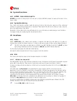
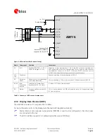
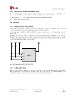
Page 20: ...XTINT1 A signal change on pins RXD1 EXTINT0 or EXTINT1 can also be used to wake up the receiver from Sleep or Backup Mode Pins RXD1 EXTINT0 and EXTINT1 are powered by the backup domain VDD_B These pin...

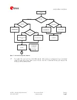
Page 21: ...No TMS CFG_PIN 1 Yes No Revert to ROM Default Safe Boot Mode Boot System Boot Safe ROM Read configuration from configuration pins CFG_xx 1 Detect Flash valid FW image with low level configuration 2 CF...

Page 22: ...12 Functional Block Configuration Sequence Once the module has started the configuration settings may be modified with UBX configuration messages The modified settings remain effective until power do...

Page 23: ...n be used which still allows taking advantage of the integrated LNA This is illustrated in Figure 13 A single ended SAW Filter F2 can be placed at the RF_IN pin fGPS 1575 42MHz SAW Filter F2 AMY 5 RF_...

Page 24: ...see the GPS Antenna Application Note 6 Schematic Plan use of 2nd interface Testpoints on serial port DDC or USB for firmware updates or as a service connector For optimal power consumption run AMY 5M...

Page 25: ...ort LDO PIO23 CFG_GPS2 V_RESET V_TH VDD_3V optional leave VDDUSB open if USB port is not used optional connect RXD1 to VDDB or GND if UART is not required PIO19 CFG_COM0 PIO21 CFG_GPS0 Figure 14 Block...

Page 26: ...E Leave open if not used C9 PIO21 CFG_GPS0 SCK GPSMON2 I O Configuration Leave open if not used D1 PIO7 EXTINT0 I External Interrupt Time Mark Pull up resistor to VDDIO If not used connect to VDDB or...

Page 27: ...pt as short as possible Assure low serial resistance in V_DCDC power supply line choose a line width 400um Keep power supply line as short as possible Design a guard ring around the optional RTC cryst...

Page 28: ...t to the receiver as well as grounding shielding and jamming from other digital devices are crucial issues and need to be considered very carefully 2 8 1 Footprint Figure 15 Recommended footprint 2 8...

Page 29: ...section Make sure that RF critical circuits are clearly separated from any other digital circuits on the system board To achieve this position the receiver digital part towards your digital section o...

Page 30: ...a USB connection The data lines between I O pins from VDD_USB to VBUS pin and from GND plane to GND pin should be as short as possible ESD Protection Device VBUS DP DM GND USB Device Connector VDD_US...

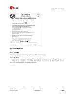
Page 31: ...ckaging TBD AMY 5M modules are delivered as hermetically sealed reeled tapes in order to enable efficient production production lot set up and tear down Figure 19 Reeled AMY 5M modules 3 1 1 Reels AMY...

Page 32: ...ection may destroy or damage them permanently According to JEDEC ISP AMY 5M modules are moisture sensitive devices Appropriate handling instructions and precautions are summarized in Sections 3 2 2 to...

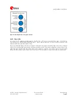
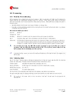
Page 33: ...3 Storage Shelf life in sealed bag is 12 months at 40 C and 90 relative humidity 3 2 4 Handling A humidity indicator card and a desiccant bag to absorb humidity are enclosed in the sealed package The...

Page 34: ...ity conditions 30 C 60 relative humidity the parts must be processed and soldered within this specified period of time Once the sealed package of the reel is opened and the parts exposed to humidity t...

Page 35: ...of bag and use a vacuum hot barrier sealing machine for sealing if not processed within specified floor time Storage in a nitrogen cabinet or dry box is also a possible approach to prevent moisture in...

Page 36: ...ly if performed excessively fine balls and large balls will be generated in clusters End Temperature 150 200 C If the temperature is too low non melting tends to be caused in areas containing large he...

Page 37: ...max 20 40 s Typical Leadfree Soldering Profile End Temp 150 200 C max 3 C s C Figure 24 Recommended soldering profile When soldering leadfree u blox 5 modules in a leaded process check the following...

Page 38: ...Ultrasonic cleaning will permanently damage the module in particular the quartz oscillators The best approach is to use a no clean soldering paste and eliminate the cleaning step after the soldering 3...

Page 39: ...OEM is strongly advised to qualify such processes in combination with the AMY 5M module before implementing this in the production Casting will void the warranty 3 3 12 Grounding Metal Covers Attempts...

Page 40: ...e local GND i e the work table and the PCB GND then the first point of contact when handling the PCB shall always be between the local GND and PCB GND GND Local GND When handling the RF pin do not com...

Page 41: ...test the sensitivity of a GPS device is with the use of a 1 channel GPS simulator It assures reliable and constant signals at every measurement Figure 25 1 channel GPS simulator u blox recommends the...

Page 42: ...he best test is to bring the device to an outdoor position with excellent sky view HDOP 3 0 Let the receiver acquire satellites and compare the signal strength with a Golden Device As the electro magn...

Page 43: ...erence Design A 1 Minimum Bill of Material The following reference design is for a smart antenna with a minimum BOM For this design u blox provides a complete Reference Design Package including Schema...

Page 44: ...AMY 5M Hardware Integration Manual Objective Specification Reference Design GPS G5 MS5 08207 Page 44 your position is our focus A 1 1 Schematic Figure 27 AMY 5 Minimum BOM Smart Antenna Schematic...

Page 45: ...CER X5R 0402 2U2 20 6 3V ROHS C2 CAP CER X5R 0402 2U2 20 6 3V ROHS C7 CAP CER X5R 0402 2U2 20 6 3V ROHS FB1 FERRITE BEAD MURATA BLM15HD 0402 1000R 100MHZ ROHS J1 DO NOT INSTALL J2 DO NOT INSTALL J3 D...

Page 46: ...sign and supports AMY 5 modules on one PCB and features one serial port as well as a USB connection If USB is not needed some components can be spared For this design u blox provides a complete Smart...

Page 47: ...AMY 5M Hardware Integration Manual Objective Specification Reference Design GPS G5 MS5 08207 Page 47 your position is our focus A 2 1 Schematic Figure 31 AMY 5 Smart Antenna Schematic...

Page 48: ...7N 5 300MA ROHS L2 IND MURATA LQW15A 0402 8N2 3 540MA ROHS L3 IND MURATA LQW15A 0402 33N 3 260MA ROHS L4 IND MURATA LQW15A 0402 22N 3 310MA ROHS L5 IND MURATA LQW15A 0402 6N8 3 700MA ROHS R11 RES THIC...

Page 49: ...AMY 5M Hardware Integration Manual Objective Specification Reference Design GPS G5 MS5 08207 u blox proprietary Page 49 A 2 3 Layout Figure 32 Pad Top Figure 33 Pad Bottom...

Page 50: ...ifications 1 1 Oscillation mode Fundamental Mode 1 2 Nominal frequency at 25 C 32 768 kHz 1 3 Frequency calibration tolerance at 25 C 100 ppm 2 Electrical Specifications 2 1 Load capacitance CL 9 pF 2...

Page 51: ...dard Capacitors Name Use Type Value C1 RF input DC block COG 47P 5 25V C Decoupling Supply Capacitor X5R 2U2 20 6 3V C19 Load capacitor XTAL_IN COG 12P 5 25V C20 Load capacitor XTAL_OUT COG 12P 5 25V...

Page 52: ...bjective Specification Component Selection GPS G5 MS5 08207 u blox proprietary Page 52 Name Use Type Value R38 Antenna supervisor voltage divider 560R 5 0 1W R39 Antenna supervisor voltage divider 100...

Page 53: ...on to the NMEA protocol PVT Position Velocity Time SA Selective Availability SV Satellite Vehicle SBAS Satellite Based Augmentation Systems UBX File extension for u center log file or short form for t...

Page 54: ...x com Technical Support Phone 41 44 722 74 44 E mail info u blox com Asia Australia Pacific u blox Singapore Pte Ltd 435 Orchard Road 17 01 Wisma Atria Singapore 238877 Phone 65 6734 3811 Fax 65 6736...

Reviews: