your position is our focus
ANTARIS
GPS module
micro strip line
O tional active antenna supply
p
As
seen
in
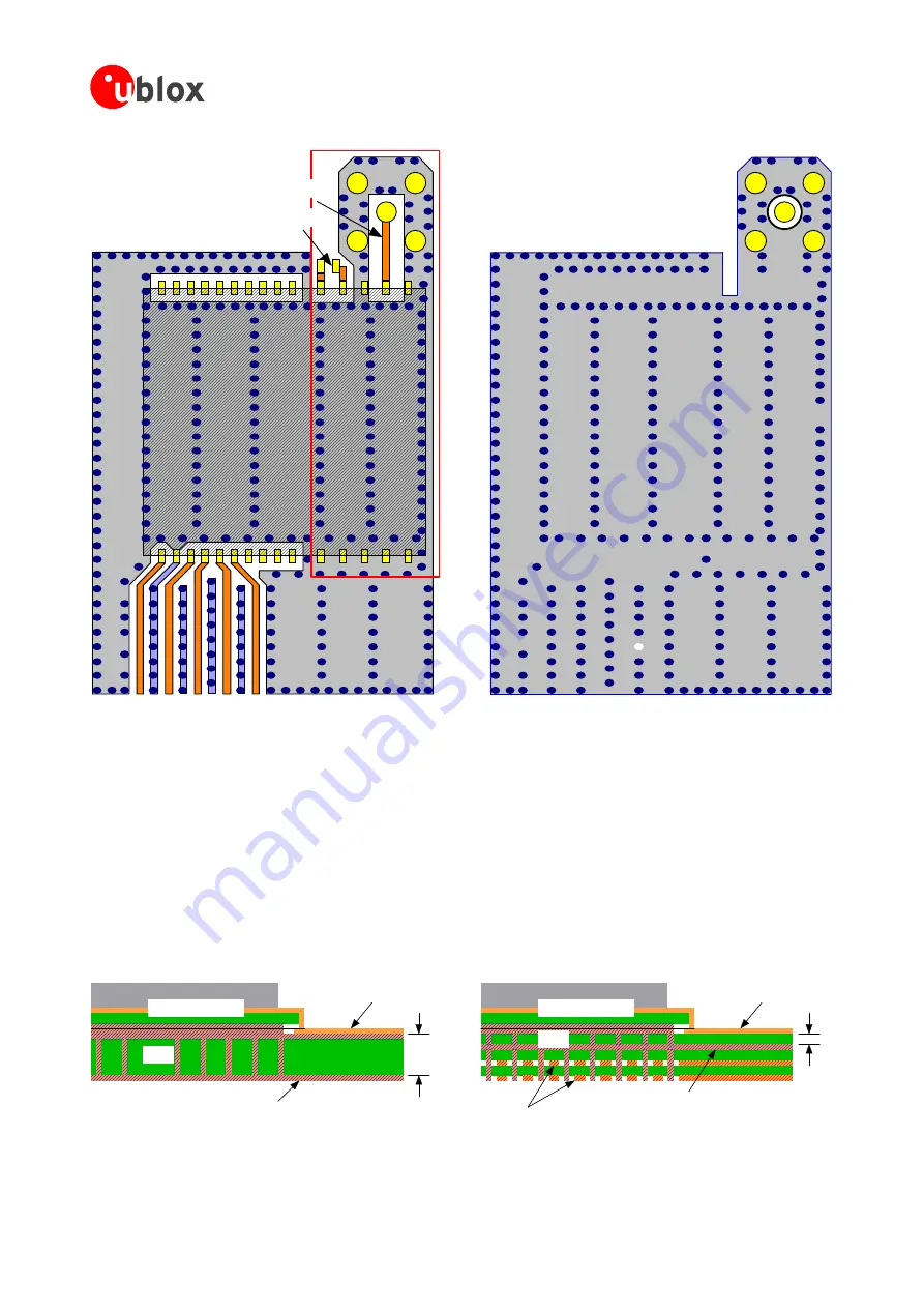
Figure 43,
an
isolated
ground
area
is
created
around
and
below
the
RF
connection.
This
part
of
the
potential
noise
sources
as
possible.
Make
sure
that
no
signal
lines
cross
or
a
B
and
a
4
Layer
PCB.
The
reference
ground
Figure 43: Recommended layout for TIM-xx
circuit
has
to
be
kept
as
far
away
from
vias
of
signal
traces
show
up
at
the
PCB
surface
underneath
the
area
surrounded
by
the
red
rectangle.
Also,
the
ground
plane
should
be
free
from
digital
supply
return
currents
in
this
area.
On
a
multi
layer
board,
the
whole
layer
stack
below
the
RF
connection
should
be
free
of
digital
lines.
This
is
because
even
a
solid
ground
plane
provides
only
limited
isol tion.
The
impedance
of
the
antenna
connection
has
to
match
the
50
Ohm
impedance
of
the
receiver.
To
achieve
an
impedance
of
50
Ohms,
the
width
W
of
the
micro
strip
has
to
be
chosen
depending
on
the
dielectric
thickness
H,
the
dielectric
constant
ε
r
of
the
dielectric
material
of
the
PCB
and
on
the
build-up
of
the
PCB
(see
Section 3.6.5
).
Figure 44
shows
two
different
builds:
A
2
Layer
PC
plane
is
in
both
designs
on
layer
2
(red).
Therefore
the
effective
thickness
of
the
dielectric
is
different.
GPS Module
micro strip line
Ground plane
GPS Module
micro strip line
Ground plane
PCB
PCB
Either don't use these layers or fill with ground planes
H
H
Figure 44: PCB build-up for Micro strip line. Left: 2-layer PCB, right: 4-layer PCB
GPS
Modules
-
System
Integration
Manual
(SIM)
(incl.
Reference
Design)
Design-In
GPS.G4-MS4-05007-A1
Page 55


