


C030-R412M - User Guide
UBX-19010121 - R01
Hardware description
Page 18 of 27
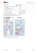
2.6
Test, break out points, and debug interfaces
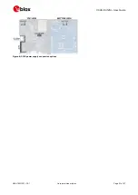
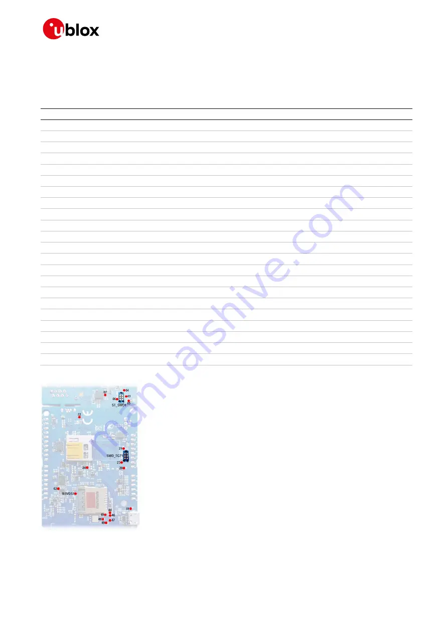
The C030-R412M has test and break out points to access key signals of the circuitry as well as
interface and Host MCU debug interfaces placed on the bottom side of the PCB for easy access. These
are listed in
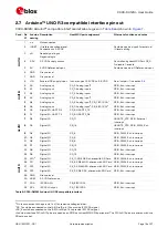
Name
Signal
01
Cellular module supply voltage
02
GNSS module supply voltage
03
InterfaceMCU SWDCLK
04
InterfaceMCU SWDIO
05
InterfaceMCU reset
06
3.3 VDC supply for InterfaceMCU
07
OE signal for IC4 level translator between utility and application sections
08 to 19
N/A
20
1.8VDC supply for Host MCU
21
Host MCU SWDIO
22
Host MCU Reset
23
Host MCU SWDCLK
24
Host MCU BOOT0
44
Cellular module pin 44 break-out (SPK_P). Unused
45
Cellular module pin 45 break-out (SPK_N). Unused
46
Cellular module pin 46 break-out (MIC_BIAS). Unused
47
Cellular module pin 47 break-out (MIC_GND). Unused
48
Cellular module pin 48 break-out (MIC_N). Unused
49
Cellular module pin 49 break-out (MIC_P). Unused
RSVDS1
Cellular module pin 19 break-out (RSVD, Reserved). Unused
ST-SWD1
Tag-Connect-NL Plug-of-Nails™ connector compatible PCB touch points footprint for Interface MCU
SWD_TGT1
Tag-Connect-NL Plug-of-Nails™ connector compatible PCB touch points footprint for Host MCU
Table 5: C030-R412M test and break out points and debug interfaces
Figure 6: C030-R412M test and break out points and debug interfaces (bottom view)


