


C030-R412M - User Guide
UBX-19010121 - R01
Hardware description
Page 8 of 27
2.1
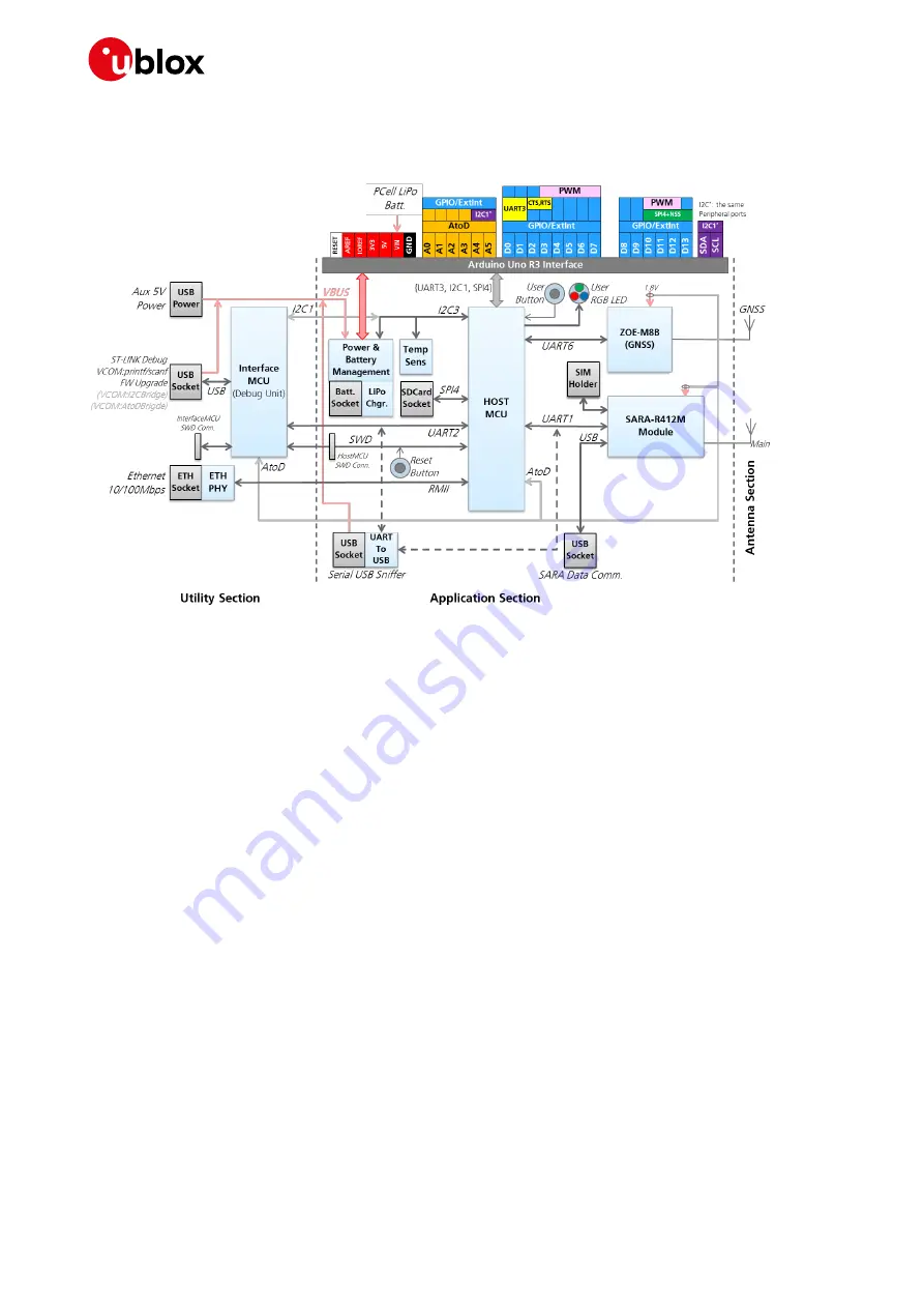
C030-R412M block diagram
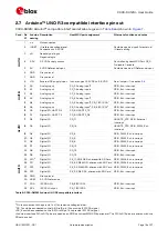
shows the block diagram of the C030-R412M.
Figure 2: C030-R412M block diagram
shows the major interfaces and internal connections of the C030-R412M.
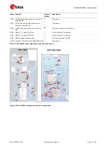
The major component layout of the board is provided in
The C030-R412M consists of three sections:
Utility section
The utility section accommodates the components that provide SW debugging / virtual COM port
(ST-Link/CMSIS-DAP) and Ethernet Interface functions. The SW debugging / virtual COM port
functions are executed by the InterfaceMCU via the “Debug USB” interface.
As this section is only needed during the application development and test activities, it could be
physically snapped off from the application section to decrease the size and power consumption.
The utility section is powered up from the “Debug USB” 5V VBus. When the “Debug USB” is not
connected, SW debugging / virtual COM port and Ethernet Interface functions are turned off and
isolated from the application section.
The “Auxiliary 5V USB” connector on the utility section could be used to boost the power input to the
application section if the current input from the “Debug USB” 5V Vbus is not sufficient.
Application section
The application section accommodates the GNSS and cellular modules, a eUICC (Embedded SIM) /
MicroSIM socket, the HostMCU, the battery charging/management and power supply circuitry, the
SD card interface and socket, the Serial USB sniffer for communication between the HostMCU to the
cellular module and similarly to the InterfaceMCU. The application section also has a temperature
sensor for measuring ambient temperature of the board. Reset and user buttons, configuration
jumpers and User and system status indication LEDs are placed in the application section.
VSYS


