LARA-R2 series - System Integration Manual
UBX-16010573 - R02
Objective Specification
Design-in
Page 70 of 148
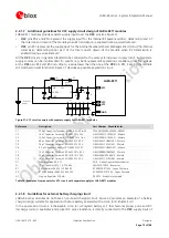
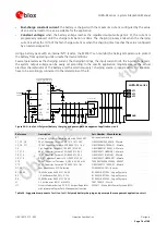
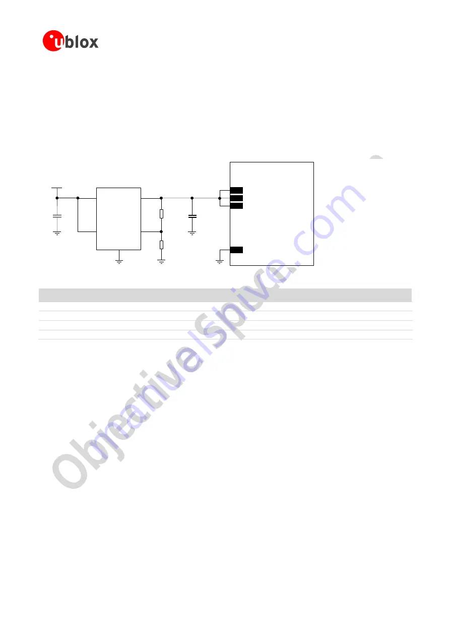
Figure 29 and the components listed in Table 22 show an example of a low cost power supply circuit, where the
VCC
module supply is provided by an LDO linear regulator capable of delivering the specified highest peak /
pulse current, with proper power handling capability. The regulator described in this example supports a limited
input voltage range and it includes internal circuitry for current and thermal protection.
It is recommended to configure the LDO linear regulator to generate a voltage supply value slightly below the
maximum limit of the module VCC normal operating range (e.g. ~4.1 V as in the circuit described in Figure 29
and Table 22). This reduces the power on the linear regulator and improves the whole thermal design of the
supply circuit.
5V
C1
IN
OUT
ADJ
GND
1
2
4
5
3
C2
R1
R2
U1
EN
LARA-R2 series
52
VCC
53
VCC
51
VCC
GND
Figure 29: Example of low cost VCC supply application circuit using an LDO linear regulator
Reference
Description
Part Number - Manufacturer
C1, C2
10 µF Capacitor Ceramic X5R 0603 20% 6.3 V
GRM188R60J106ME47 - Murata
R1
27 k
Resistor 0402 5% 0.1 W
RC0402JR-0727KL - Yageo Phycomp
R2
4.7 k
Resistor 0402 5% 0.1 W
RC0402JR-074K7L - Yageo Phycomp
U1
LDO Linear Regulator ADJ 3.0 A
LP38501ATJ-ADJ/NOPB - Texas Instrument
Table 22: Components for low cost VCC supply application circuit using an LDO linear regulator

