background image

MAX-7 / NEO-7 / LEA-7 - Hardware Integration Manual 

GPS.G7-HW-11006-1 


Migration to u-blox-7 modules 


Page 37 of 55


4


Migration to u-blox-7 modules 

4.1


Migrating u-blox 6 designs to a u-blox 7 module 

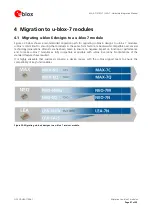
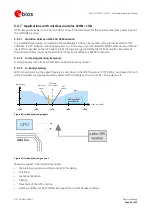
Figure 33  below shows a recommended migration path for migrating u-blox 6 designs to u-blox 7 modules. 
u-blox is committed to ensuring that products in the same form factor are backwards compatible over several 
technology generations. Utmost care has been taken to ensure no negative impact on function or performance 
and to make u-blox 7 modules as fully compatible  as possible with u-blox 6 versions. No  limitations  of the 
standard features have resulted. 
It is highly advisable that  customers consider a design review with the u-blox support team to ensure the 
compatibility of key functionalities.    


Figure 33: Migrating u-blox 6 designs to a u-blox 7 receiver module 

Summary of Contents for LEA-7 Series

Page 1: ...u blox 7 positioning engine These compact easy to integrate stand alone GPS GNSS receiver modules combine exceptional GPS GNSS performance with highly flexible power design and connectivity options Th...

Page 2: ...to the following products Name Type number ROM FLASH version PCN reference MAX 7C 0 All ROM1 00 MAX 7Q 0 All ROM1 00 MAX 7W 0 All ROM1 00 NEO 7N 0 All FLASH1 00 NEO 7M 0 All ROM1 00 LEA 7N 0 All FLAS...

Page 3: ...are Integration Manual provides the necessary information to successfully design in and configure these u blox 7 based positioning modules For navigating this document please note the following This m...

Page 4: ...email Use our service pool email addresses rather than any personal email address of our staff This ensures that we process your request as soon as possible You will find the contact details at the e...

Page 5: ...2 6 1 UART 11 2 6 2 USB 11 2 6 3 Display Data Channel DDC 13 2 6 4 SPI NEO 7 13 2 7 I O pins 13 2 7 1 RESET_N Reset input 13 2 7 2 EXTINT External interrupt 13 2 7 3 D_SEL Interface select NEO 7 14 2...

Page 6: ...e migration NEO 6 NEO 7 39 4 2 3 Hardware migration MAX 6 MAX 7 40 4 2 4 Hardware migration LEA 6N LEA 7N 41 4 3 Software migration 42 4 3 1 Software compatibility 42 4 3 2 Messages no longer supporte...

Page 7: ...tegration Manual GPS G7 HW 11006 1 Contents Page 7 of 55 6 3 1 Guidelines for sensitivity tests 52 6 3 2 Go No go tests for integrated devices 52 Appendix 53 A Abbreviations 53 Related documents 53 Re...

Page 8: ...actors in leadless chip carrier LCC packages they are easy to integrate and combine exceptional positioning performance with highly flexible power design and connectivity options SMT pads allow fully...

Page 9: ...e ANT_ON signal in order to optimize power consumption see section 2 7 5 Using the USB Interface is not recommended with Power Save Mode since the USB standard does not allow a device to be non respon...

Page 10: ...BCKP pin to VCC_IO or to VCC if not avaiable As long as the u blox 7 module is supplied to VCC and VCC_IO the backup battery is disconnected from the RTC and the BBR to avoid unnecessary battery drain...

Page 11: ...evice to the host The VDD_USB pin supplies the USB interface u blox provides Microsoft certified USB drivers for Windows XP Windows Vista and Windows 7 operating systems also Windows 8 compatible Thes...

Page 12: ...the peak supply current see a low cost DC DC converter such as LTC3410 from Linear Technology C23 C24 Capacitors Required according to the specification of LDO U1 D2 Protection diodes Protect circuit...

Page 13: ...er every byte is read from register 0xFF the internal address counter is incremented by one saturating at 0xFF Therefore subsequent reads can be performed continuously 2 6 4 SPI NEO 7 With NEO 7 modul...

Page 14: ...Implementation and Aiding Features in u blox wireless modules 10 2 7 5 ANT_ON Antenna ON LNA enable NEO 7N MAX 7Q MAX 7C In Power Save Mode the system can turn on off an optional external LNA using t...

Page 15: ...er supply any resistance in the VCC supply line can negatively influence performance Consider the following points o Wide power lines or even power planes are preferred o Avoid resistive components in...

Page 16: ...multi layer PCB use the thickness of the dielectric between the signal and the first GND layer typically the 2nd layer for the micro strip calculation If the distance between the micro strip and the a...

Page 17: ...ration Manual GPS G7 HW 11006 1 Design Page 17 of 55 3 2 1 Minimal design NEO 7N This is a minimal setup for a GPS GNSS receiver with a NEO 7N module Figure 5 NEO 7 passive antenna design For active a...

Page 18: ...al active antenna UART TxD 20 O Serial Port SPI MISO Communication interface Can be programmed as TX ready for DDC interface If pin 2 low SPI MISO RxD 21 I Serial Port SPI MOSI Serial input Internal p...

Page 19: ...ed for active antenna or external LNA supply ANT_ON MAX 7C Q Reserved MAX 7W 13 O ANT_ON Active antenna or ext LNA control pin in power save mode ANT_ON pin voltage level is VCC_IO Reserved Leave open...

Page 20: ...to VCC VDD_USB 24 I USB Power Supply To use the USB interface connect this pin to 3 0 3 6V If no USB serial port used connect to GND Antenna RF_IN 16 I GPS GALILEO signal input from antenna Use a con...

Page 21: ...GPS GNSS system GPS GNSS signals at the surface of the Earth are about 15 dB below the thermal noise floor Signal loss from the antenna to RF_IN pin of the module must be minimized as much as possible...

Page 22: ...0 8 mm Consider the paste mask outline when defining the minimal distance to the next component The exact geometry distances stencil thicknesses and solder paste volumes must be adapted to the specifi...

Page 23: ...sheet 3 3 3 Antenna connection and ground plane design u blox 7 modules can be connected to passive or active antennas The RF connection is on the PCB and connects the RF_IN pin with the antenna feed...

Page 24: ...with ground planes H H Figure 16 PCB build up for micro strip line Left 2 layer PCB right 4 layer PCB 3 3 4 General design recommendations The length of the micro strip line should be kept as short a...

Page 25: ...e 19 As a rule of thumb to achieve a 50 line impedance with FR 4 material the width of the conductor is roughly double the thickness of the dielectric Note For the correct calculation of the micro str...

Page 26: ...50 3 4 1 1 Minimal setup with a good patch antenna Figure 20 shows a minimal setup for a design with a good GPS patch antenna NEO 7N is optimized for Immunity to near field Wireless Figure 20 Module d...

Page 27: ...tive antenna In case of different supply voltage use a filtered external supply as shown in section 3 4 2 2 3 4 2 1 Active antenna design VCC_RF used to supply active antenna Figure 22 shows an active...

Page 28: ...the state diagram below Figure 24 The current active antenna status can be determined by polling the UBX MON HW monitor command If an antenna is connected the initial state after power up is Active An...

Page 29: ...pervisor is not configured and deactivated ANTSTATUS OK Active antenna connected and powered ANTSTATUS SHORT Antenna short ANTSTATUS OPEN Antenna not connected or antenna defective Table 8 Active ante...

Page 30: ...tion see data sheet For recomended parts see section 3 5 External supply LEA 7N MAX 7W Figure 26 shows an externally powered active antenna design Since the external bias voltage is fed into the most...

Page 31: ...ee data sheet RF Vcc Rbias R R R I _ 3 2 2 Equation 1 Calculation of threshold current for open circuit detection Antenna open circuit detection OCD is not activated by default on the MAX 7 module OCD...

Page 32: ...ON RF Vcc R R R R I bias _ 3 2 2 Equation 2 Calculation of threshold current for open circuit detection For recomended parts see section 3 5 3 4 3 5 External active antenna control NEO 7N MAX 7Q MAX 7...

Page 33: ...tenna accordingly to let both signals pass Figure 30 GPS GLONASS SAW filter Usually an active GPS antenna includes a GPS band pass filter which may filter out the GLONASS signal see Figure 30 For this...

Page 34: ...orting GLONASS have a GPS GLONASS SAW filter see Figure 30 that lets both GPS and GLONASS signals pass For best performance with passive antenna designs use an external LNA See section 3 4 1 2 Figure...

Page 35: ...58KB0F0A GPS GLONASS Low insertion loss Only for mobile application Triquint B9850 GPS Compliant to the AEC Q200 standard CTS CER0032A GPS Ceramic filter also offers robust ESD Protection LNA Avago AL...

Page 36: ...ions 2J Tallysman Wireless Table 10 Recommend GPS GLONASS active antenna A1 3 5 2 Recommended GPS GLONASS passive patch antenna Manufacturer Order No Comments Amotech www amotech co kr B35 3556920 2J2...

Page 37: ...at products in the same form factor are backwards compatible over several technology generations Utmost care has been taken to ensure no negative impact on function or performance and to make u blox 7...

Page 38: ...TxD RxD VCC_RF SDA and SCL Changes SPI implementation has changed With u blox 6 SPI uses pins 2 14 15 16 With u blox 7 SPI is available on pins 18 19 20 21 when pin 2 set low See Table 14 Not supporte...

Page 39: ...13 GND GND GND GND No difference 14 MOSI CFG_ COM0 SPI MOSI Configuration Pin Leave open if not used ANT_ON turn on and off an optional external LNA ANT_ON antenna on can be used to turn on and off an...

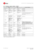
Page 40: ...7 3 6V VCC Power supply of module MAX 7C 1 65 3 6V MAX 7Q 2 7 3 6V 9 VRESET connect to pin 8 RESET_N Reset input With MAX 6 if Reset input is used it implements the 3k3 resistor from pin 9 to pin 8 T...

Page 41: ...to do the same in u blox 7 12 Reserved Do not drive low Reserved Do not drive low No difference 13 GND Ground GND Ground No difference 14 GND Ground GND Ground No difference 15 GND Ground GND Ground...

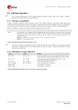
Page 42: ...cating with u blox wireless modules this change of pins is not recognized by LEON FW7 60 02 and previous versions u blox 6 0 s leap second by default FW 6 02 and FW7 0x 15 s leap second by default u b...

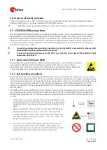
Page 43: ...low precise control of the temperature and all parts will be heated up evenly regardless of material properties thickness of components and surface color Consider the IPC 7530 Guidelines for temperatu...

Page 44: ...not be easily removed with a washing process Cleaning with water will lead to capillary effects where water is absorbed in the gap between the baseboard and the module The combination of residues of s...

Page 45: ...dule Always avoid overheating the module After the module is removed clean the pads before placing and hand soldering a new module Never attempt a rework on the module itself e g replacing individual...

Page 46: ...other industries to describe momentary unwanted currents that may cause damage to electronic equipment 5 3 2 ESD handling precautions ESD prevention is based on establishing an Electrostatic Protecti...

Page 47: ...rmance sufficient Active antennas A RF_IN GPS Receiver LNA B L RF_IN GPS Receiver C D RF_IN GPS Receiver LNA with appropriate ESD rating Figure 35 ESD Precautions Protection measure A is preferred bec...

Page 48: ...ollowing elements are critical regarding EMI Unshielded connectors e g pin rows etc Weakly shielded lines on PCB e g on top or bottom layer and especially at the border of a PCB Weak GND concept e g s...

Page 49: ...lters from Epcos B9444 or B7839 or Murata 5 3 7 2 Increasing jamming immunity Jamming signals come from in band and out band frequency sources 5 3 7 3 In band jamming With in band jamming the signal f...

Page 50: ...0 500 1000 1500 2000 GPS input filter characteristics 0 110 0 500 1500 2000 Frequency M Hz GSM 900 GSM 1800 GSM 1900 Pow er dBm GPS input filter characteristics GPS 1575 0 110 GPS signals GSM 950 Fig...

Page 51: ...e done Digital self test Software Download verification of FLASH firmware etc Measurement of voltages and currents Measurement of RF characteristics e g C No Traceability down to component level X Ray...

Page 52: ...product 2 Choose the power level in a way that the Golden Device would report a C No ratio of 38 40 dBHz 3 Power up the DUT Device Under Test and allow enough time for the acquisition 4 Read the C No...

Page 53: ...tions used Related documents 1 NEO 7 Data Sheet Docu No GPS G7 HW 11004 2 MAX 7 Data Sheet Docu No GPS G7 HW 12012 3 LEA 7N Data Sheet Docu No GPS G7 HW 12039 4 u blox 7 Receiver Description including...

Page 54: ...age 54 of 55 Revision history Revision Date Name Status Comments September 4 2012 jfur Initial draft 1 December 20 2012 jfur MAX 7W added Revision Chapter 3 4 Antenna supervision DC bloc removed from...

Page 55: ...blox AG Phone 41 44 722 74 44 E mail info u blox com Technical Support Phone 41 44 722 74 44 E mail support u blox com Asia Australia Pacific u blox Singapore Pte Ltd Phone 65 6734 3811 E mail info_a...

Reviews: