LILY-W1 series - System integration manual
UBX-15027600 - R09
Design-in
Page 17 of 64
C1 - Public
o
FR-4 material exhibits poor thickness stability and thus less control of impedance over
the trace length. Contact the PCB manufacturer for specific tolerance of controlled
impedance traces.
•
For PCBs using components bigger than 0402 and dielectric thickness below 200
µ
m, it is
recommended to add a keep-out (that is, clearance, a void area) on the ground reference layer
below any pin present on the RF transmission lines to reduce parasitic capacitance to ground.
•
The transmission lines width and spacing to GND must be uniform and routed as smoothly as
possible: route RF lines in 45 ° angle.
•
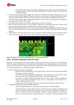
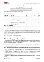
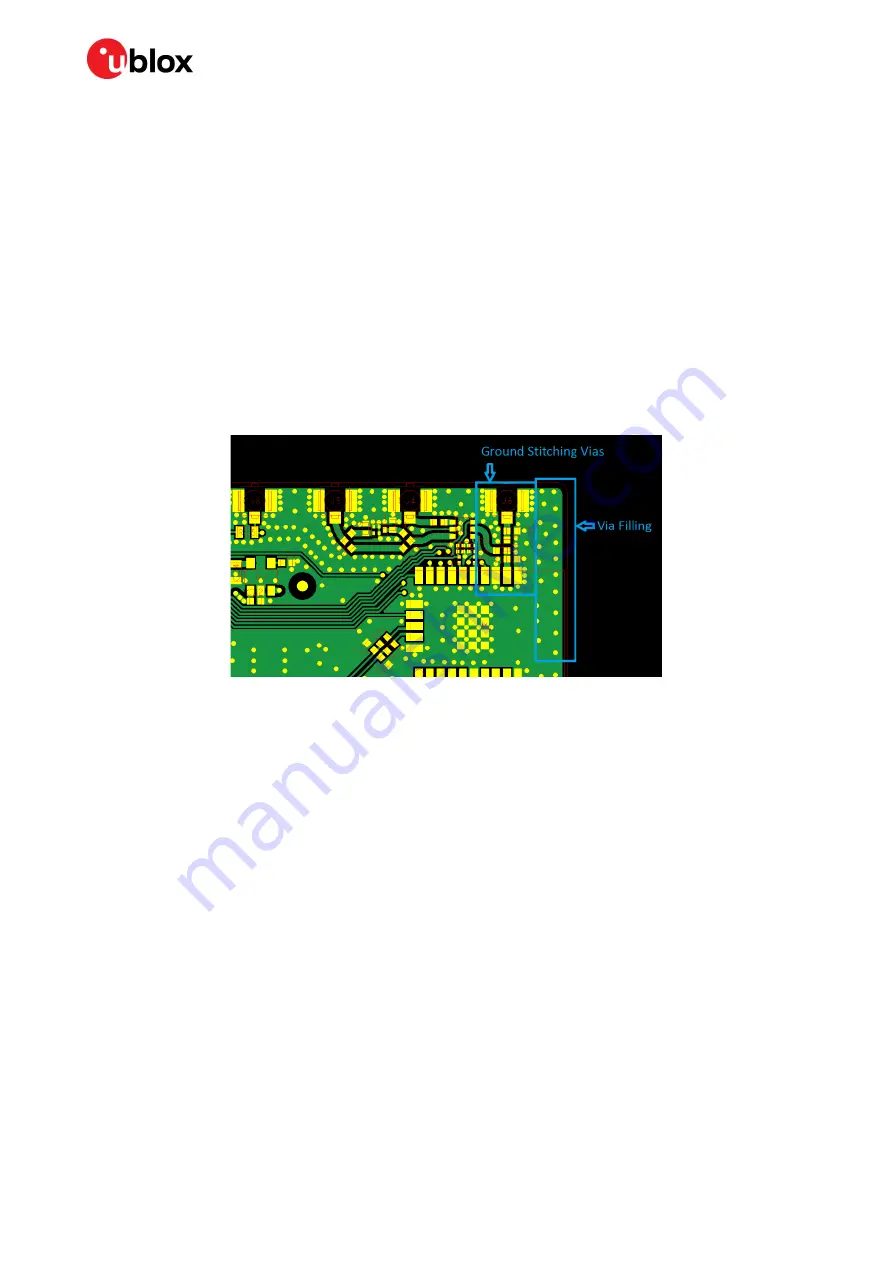
Add GND stitching vias around transmission lines as shown in Figure 5.
•
Ensure solid metal connection of the adjacent metal layer on the PCB stack-up to main ground
layer, providing enough vias on the adjacent metal layer as shown in Figure 5.
•
Route RF transmission lines far from any noise source (as switching supplies and digital lines) and
from any sensitive circuit to avoid crosstalk between RF traces and Hi-impedance or analog
signals.
•
Avoid stubs on the transmission lines, any component on the transmission line should be placed
with the connected pin over the trace. Also avoid any unnecessary component on RF traces.
Figure 5: Example of RF trace and ground design from LILY-W1 Evaluation Kit (EVK)
2.2.2
Antenna design (LILY-W131 only)
Designers must take care of the antennas from all perspective at the very start of the design phase
when the physical dimensions of the application board are under analysis/decision, since the RF
compliance of the device integrating LILY-W1 module with all the applicable required certification
schemes heavily depends on antennas radiating performance.
•
External antennas such as linear dipole:
o
External antennas basically do not imply physical restriction to the design of the PCB
where the module is mounted.
o
The radiation performance mainly depends on the antennas. It is required to select
antennas with optimal radiating performance in the operating bands.
o
RF cables should be carefully selected with minimum insertion losses. Additional
insertion loss will be introduced by low quality or long cable. Large insertion loss
reduces radiation performance.
o
A high quality 50
Ω
coaxial connector provides proper PCB-to-RF cable transition.
•
Integrated antennas such as patch-like antennas:
o
Internal integrated antennas imply physical restriction to the PCB design:
Integrated antenna excites RF currents on its counterpoise, typically the PCB ground
plane of the device that becomes part of the antenna; its dimension defines the
minimum frequency that can be radiated. Therefore, the ground plane can be reduced
down to a minimum size that should be similar to the quarter of the wavelength of the


