LILY-W1 series - System integration manual
UBX-15027600 - R09
Appendix
Page 59 of 64
C1 - Public
B.1.1 Floor plan and PCB stack-up
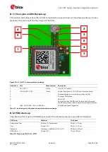
This section describes where the critical components are positioned on the reference design. It also
presents the stack-up of the four layers of the PCB.
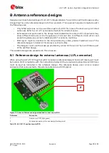
Figure 18: LILY-W131 antenna reference design
Reference Part
Manufacturer Description
1
LILY-W131
u-blox
LILY-W131 module
2
U.FL-R-SMT-1(10)
Hirose
Coaxial Connector, 0 – 6 GHz, for external antenna
3
Antenna coplanar microstrip, matched to 50
Ω
4
Top layer GND-plane
5
Host PCB.
Should have a solid GND inner layer under and around
the RF components (vias and small openings is allowed).
6
10pF, COG, 0402, 10P +/-0.25P 25V
Antenna connector capacitor
Table 31: Included part in the antenna connector reference design
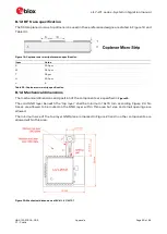
B.1.2 PCB stack-up
The stack-up from top to solid GND layer used in the reference design is specified in Table 32.
PCB Layer
Material
Thickness
Soldermask Top
Generic LPI Soldermask
20 µm +/-10 µm
Top
Copper Foil
35 µm +/-15 µm
Dielectric
Pre-preg,
ε
r @2GHz: 4.05 +/-0.15
300 µm +/-40 µm
GND plane
Copper Foil
15 µm +30 µm
Table 32: Stack-up of EVK-LILY-W131
2
3
1
4
6
5
4
3

