NINA-B4 series - System integration manual
UBX-19052230 - R06
Functional description
Page 7 of 45
C1-Public
1.3
Block diagrams
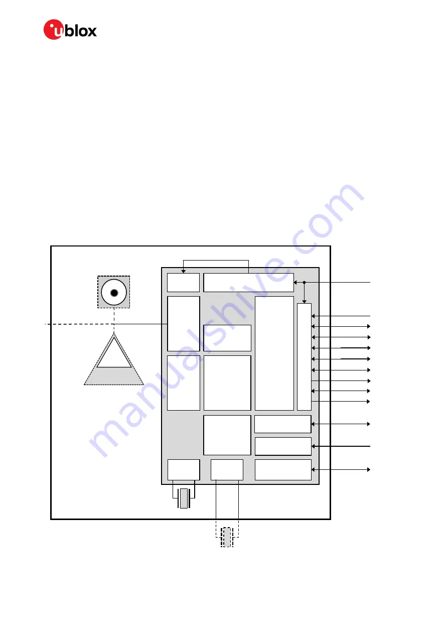
Block diagrams of the NINA-B40 and NINA-B41 module designs are shown in Figure 1 and Figure 2.
1.3.1
NINA-B40
A block diagram of the NINA-B40 open-cpu module design showing the alternative U.FL connector
(B400), antenna pin (B401), and PCB trace antenna (B406) solutions is shown in Figure 1.
☞
NINA-B400 modules include a U.FL connector for connecting an external antenna. The module size
is 10 x 15 x 2.2 mm.
☞
NINA-B401 modules include an ANT pad on the footprint for connecting an external antenna. The
module size is 10 x 11.6 x 2.2 mm.
☞
NINA-B406 module support an internal PCB trace antenna using antenna technology from Proant
AB. The module size is 10 x 15 x 2.2 mm.
Figure 1: NINA-B40 series block diagram
DC/DC and LDO regulators
512 kB flash
Bluetooth LE
baseband
IO
bu
ff
ers
A
rm
®
C
o
rtex®
-M
4
w
it
h
FP
U
PLL
VCC_IO (1.7 – 3.6 V)
VCC (1.7 – 3.6 V)
32 MHz
Reset
2x UART
SPI
GPIO
1.3 V
System
power
I2C
PWM
I2S
ADC and
comparator
Analog
Passive NFC tag
NFC
128 kB
RAM
PLL
32.768 kHz
RTC, timers
and counters
RF
Nordic Semiconductor
nRF52833
USB device
USB 2.0
QDEC
PDM
(NINA-B406)
PCB trace antenna
(NINA-B400)
U.FL antenna connector
(NINA-B401)
Antenna pin


