background image


NORA-W30 series - System integration manual 

UBX-22021119 - R02 

Handling and soldering


Page 32 of 52 

C1-Public  


5


Handling and soldering 


NORA-W30 series modules are Electrostatic Sensitive Devices that demand the 
observance  of  special  handling  precautions  against  static  damage.  Failure  to 
observe these precautions can result in severe damage to the product.  

5.1


ESD handling precautions 

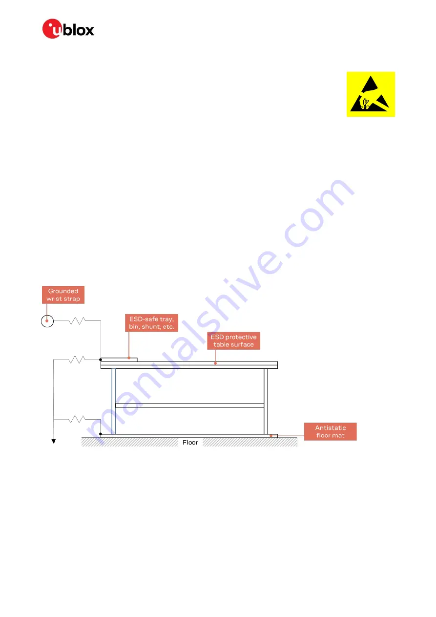
As the risk of electrostatic discharge in the RF transceivers and patch antennas of the module is of 
particular concern, standard ESD safety practices are prerequisite. See also 

Figure 7

. 

Consider also: 


When connecting test equipment or any other electronics to the module (as a standalone or PCB-
mounted device), the first point of contact must always be to local GND. 


Before mounting an antenna patch, connect the device to ground. 


When  handling  the  RF  pin,  do  not  touch  any  charged  capacitors.  Be  especially  careful  when 
handling materials like patch antennas (~10 pF), coaxial cables (~50-80 pF/m), soldering irons, or 
any other materials that can develop charges. 


To prevent electrostatic discharge through the RF input, do not touch any exposed antenna area. 
If there is any risk of the exposed antenna being touched in an unprotected ESD work area, be sure 
to implement proper ESD protection measures in the design. 


When soldering RF connectors and patch antennas to the RF pin on the receiver, be sure to use an 
ESD-safe soldering iron (tip). 


Figure 7: Standard workstation setup for safe handling of ESD-sensitive devices 

5.2


Packaging, shipping, storage, and moisture preconditioning 

For information pertaining to reels, tapes or trays, moisture sensitivity levels (MSL), shipment and 
storage,  as  well  as  drying  for  preconditioning,  refer  to  the  NORA-W30  series  data  sheet

  [2]

  and 

Packaging information reference guide 

[1]

. 

Summary of Contents for NORA-W30 Series

Page 1: ...delines for integrating NORA W30 series stand alone dual band Wi Fi and Bluetooth Low Energy modules in customer applications It also describes open CPU application development solutions using the Rea...

Page 2: ...uction information Document contains the final product specification This document applies to the following products Product name Document status Comment NORA W301 Objective specification NORA W306 Ob...

Page 3: ...ply VDD 13 2 4 2 Power supply configuration 13 2 4 3 VDD application circuits 13 2 5 Module reset 14 2 5 1 nRESET pin 14 2 6 Bootstrap pins 14 2 7 Real time clock 14 2 7 1 External low frequency clock...

Page 4: ...ESD guidelines 27 3 8 Design in checklists 28 3 8 1 Schematic checklist 28 3 8 2 Layout checklist 28 4 Open CPU software 29 4 1 Wi Fi MAC and Bluetooth device addresses and other production data 29 4...

Page 5: ...ompliance pending 42 6 6 1 Taiwan NCC warning statement 42 6 6 2 Labeling requirements for end product 42 6 7 KCC South Korea compliance pending 42 6 8 Brazil compliance pending 43 6 9 Australia and N...

Page 6: ...S 1 2 1 3 encryption Bluetooth LE secure connection pairing and HTTPS NORA W30 modules have the same size and position of critical pads and interfaces as other NORA modules This offers maximum flexibi...

Page 7: ...ect state during startup See also Module reset 1 3 Pin assignment No Name I O1 Bootstrap Alternate functions A1 VSS Power A2 n c A3 n c A4 n c A5 PA 7 I O PU UART_DL UART_LOG_TXD ANT_SEL_P A6 PA 8 I O...

Page 8: ...CLK QDEC_PHA EXT_32K C9 n c D1 n c D2 n c D3 n c D7 n c D8 PB 1 I O AI LP_UART_TXD ANT_SEL_N BT_STE EN_EXLNA HS_TIM4_TRIG D9 n c E1 n c E2 n c E3 n c E4 VSS Power E5 VSS Power E7 n c E8 PB 2 I O AI LP...

Page 9: ...EN_EXPA KEY_ROW1 J9 PA 12 I O LP_UART_TXD SPI1_MOSI HS_PWM0 LP_PWM0 I2S_MCLK ANT_SEL_N GRANT_BT EN_EXLNA KEY_ROW0 K1 n c K2 VSS Power K3 VSS Power K5 VSS Power K7 VSS Power K8 VSS Power K9 ANT I O L1...

Page 10: ...TX LP_I2C_SCL HS_PWM4 LP_PWM4 HSDM MBOX_I2C_INT wlmac_dbggpio 0 KEY_COL1 PA 25 2 PA 26 PA 26 LP_UART_TXD HS_USI_SPI_MISO IR_RX LP_I2C_SDA HS_PWM5 LP_PWM5 HSDP BT_ACT wlmac_dbggpio 1 KEY_COL0 PA 26 2 P...

Page 11: ...2S_SD_TX2 O PA 14 12 External I2S data Tx2 I2S_SD_RX I PB 22 12 External I2S data Rx Table 5 External I2S pin multiplexing UBXDOC 39674697 1341 C2 Restricted NORA W30 AON pin mux Port Name Trap FUNC_I...

Page 12: ...from different external and internal inputs For more information about power modes see the Realtek RTL8720DF data sheet 3 and application note 5 2 2 1 Power on This is the normal operating mode when...
Page 13: ...ignificantly higher than the operating supply voltage of the module This offers the best power efficiency for the application design and minimizes the amount of current drawn from the main supply sour...

Page 14: ...n Table 7 Internal pull up values are the default states for NORA W30 on boot Use of boot strap pins as I O should be avoided if other GPIO pins can be used instead Pin State during boot Internal pull...

Page 15: ...s that is seen at the antenna port Matching components are often required to retune the antenna to 50 characteristic impedance It is difficult to predict the actual matching values for the antenna in...

Page 16: ...g 115 2 kbps because it is prone to buffer overruns When used in infrared mode the maximum modulation frequency is 500 kHz The LP_UART0 interface can also be used for firmware upgrade See also Open CP...

Page 17: ...2 10 2 Key scan NORA W30 modules support a keypad interface consisting of up to 5 row x 2 column or 4 row x 3 column matrices The key scan can be used to wake NORA W30 from deep sleep 2 10 3 Quadratur...

Page 18: ...gn is required to guarantee correct boot up and system operation Ensure that the voltage level is correctly defined during module boot It is important to follow the schematic and layout design recomme...

Page 19: ...ses at high frequencies can be considered in RF designs provided that o RF trace length must be minimized to reduce dielectric losses o If traces longer than a few centimeters are needed it is recomme...

Page 20: ...ennas such as patch like antennas o Internal integrated antennas imply physical restriction to the PCB design Integrated antenna excites RF currents on its counterpoise typically the PCB ground plane...

Page 21: ...ntenna interface ANT requirements for NORA W301 Observe the following recommendations while selecting external or internal antennas Select antennas that provide optimal return loss or VSWR figure over...

Page 22: ...traces that is clearance a void area in the area below the connector between the GND land pads If the connector s RF pad size is wider than the micro strip remove the GND layer beneath the RF connect...

Page 23: ...rating performance follow the instructions in this section 3 2 3 1 NORA W306 PCB trace antenna The module shall be placed in the center of an edge of the host PCB A large ground plane on the host PCB...

Page 24: ...System integration manual UBX 22021119 R02 Design in Page 24 of 52 C1 Public Figure 4 GND plane guard area enclosing NORA W3x6 Figure 5 Size of the GND cut out for the NORA W3x6 PCB trace antenna 10...

Page 25: ...ly consider the placement of the module with respect to antenna position Verify with PCB manufacturer allowable stack ups and controlled impedance dimensioning Verify that the power supply design and...

Page 26: ...GND or power High speed buses should be referenced to the ground plane If designers need to change the ground reference some capacitors should be added and an adequate number of GND vias must be adde...

Page 27: ...munity test is performed at the enclosure port defined by ETSI EN 301 489 1 as the physical boundary through which the electromagnetic field radiates If the device implements an integral antenna the e...

Page 28: ...are properly terminated A pi filter is provided in front of each antenna for final matching NORA W301 only Additional RF co location filters have been considered in the design 3 8 2 Layout checklist...

Page 29: ...2 Realtek SDK 4 2 1 FreeRTOS The Realtek SDK is based on FreeRTOS an open source real time operating system for MCUs FreeRTOS provides methods for multiple threads or tasks mutexes semaphores and soft...

Page 30: ...k_amebaD_va0_example GCC RELEASE project_hp asdk image km4_boot_all bin o Address 0x08006000 C git ambd_sdk project realtek_amebaD_va0_example GCC RELEASE project_hp asdk image km0_km4_image2 bin Flas...

Page 31: ...o Program_hp_release Select the km4_bootloader project Select Project Download Download current application Select the km4_application project Select Project Download Download current application 4 2...

Page 32: ...the device to ground When handling the RF pin do not touch any charged capacitors Be especially careful when handling materials like patch antennas 10 pF coaxial cables 50 80 pF m soldering irons or a...

Page 33: ...the thermal mass over the entire area of the fully populated host PCB the heat transfer efficiency of the oven and the type of solder paste that is used The optimal soldering profile that is used must...

Page 34: ...boards with a module populated on it Boards with combined through hole technology THT components and surface mount technology SMT devices may require wave soldering to solder theTHT components Only a...

Page 35: ...list of authorized antennas In the end product the NORA W30 series module must be installed in such a way that only authorized antennas can be used For end products using the NORA W301 the end produc...

Page 36: ...eneral RF Exposure Guidance KDB 594280 D01 Configuration Control KDB 594280 D02 U NII Device Security KDB 784748 D01 Labelling Part 15 18 Guidelines KDB 996369 D01 Module certification Guide KDB 99636...

Page 37: ...must be added to the grant file asa Class II Permissive Change 6 2 3 3 Adding a new antenna for authorization If the authorized antennas and or antenna trace design cannot be used the new antenna and...

Page 38: ...guration of the module to operate on channels 12 13 and 120 128 must be prevented accordingly The channels allowed while operating under the definition of a master or client device7 are described in T...

Page 39: ...t must be included in the end user manual or guide 9 47 CFR 2 926 Contains FCC ID XPYNORAW3 This device complies with part 15 of the FCC rules Operation is subject to the following two conditions 1 Th...

Page 40: ...0 NORA W30 is defined as either Class 1 or Class 2 radio equipment the end product integrating NORA W30 inherits the equipment class of the module Guidance on end product marking according to the RED...

Page 41: ...e following notice is applicable to Great Britain only NORA W30 series modules have been evaluated against the essential requirements of the Radio Equipment Regulations 2017 SI 2017 No 1206 as amended...

Page 42: ...tions Act The low power radio frequency devices must accept interference from legal communications or ISM radio wave radiated devices 6 6 2 Labeling requirements for end product End products based on...

Page 43: ...t be included in the end product manual 6 9 Australia and New Zealand regulatory compliance pending NORA W30 modules are compliant with the standards made by the Australian Communications and Media Au...

Page 44: ...d by the customer s local representative directly from the approval authority ICASA A sample of a NORA W30 ICASA label is shown below More information on registration as a Responsible Integrator and l...

Page 45: ...st report for each unit can be generated Figure 11 shows the ATE typically used during u blox production u blox in line production testing includes Digital self tests firmware download MAC address pro...

Page 46: ...ice The standard operational module firmware and test software on the host can be used to perform functional tests communication with the host controller check interfaces and perform basic RF performa...

Page 47: ...Purpose Input Output GUI Graphical User Interface I2C Inter Integrated Circuit I2S Inter IC Sound IDE Integrated Development Environment ISED Innovation Science and Economic Development Canada KDB Kn...

Page 48: ...niature version A connector SMT Surface Mount Technology SPI Serial Peripheral Interface TBC To Be Confirmed THT Through Hole Technology TLS Transport Layer Security UART Universal Asynchronous Receiv...

Page 49: ...able Applicable modules NORA W301 For information about how to integrate the U FL connector with the NORA W301 ANT pin see also NORA W301 U FL reference design It is necessary to follow this reference...

Page 50: ...mpedance 50 Size HxDIA 103 7 x 11 2 mm Type Hinged blade whip Connector RP SMA Comment This antenna requires to be mounted on a metal ground plane for best performance To be mounted on the U FL to Rev...

Page 51: ...or part for best performance To be connected to a U FL connector Approval13 FCC ISED RED MIC KCC ANATEL RCM NCC and ICASA ANTX100P001B24553 Manufacturer Pulse Electronics Yageo Gain 4 6 dBi 2 4 GHz 3...

Page 52: ...ctronic devices from electrostatic phenomena General requirements IEC 61340 5 1 2016 9 ETSI Electromagnetic compatibility and Radio spectrum Matters ERM ElectroMagnetic Compatibility EMC standard for...

Reviews: