SARA-G3 series - System Integration Manual
UBX-13000995 - R06
Objective Specification
Design-in
Page 139 of 218
SARA-G350
R1
IN
OUT
GND
GNSS LDO
Regulator
SHDN
u-blox GNSS
3.0 V receiver
SDA2
SCL2
R2
3V0
3V0
VMAIN
3V0
U1
23
GPIO2
SDA
SCL
C1
26
27
VCC
R3
V_BCKP
V_BCKP
2
24
GPIO3
25
GPIO4
1V8
B1
A1
GND
U2
B2
A2
VCCB
VCCA
Unidirectional
Voltage Translator
C2
C3
3V0
TxD1
EXTINT0
4
V_INT
DIR1
DIR2
OE
GNSS data ready
GNSS RTC sharing
TP
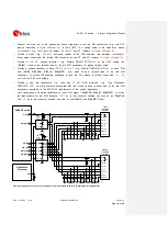
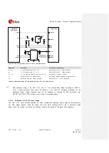
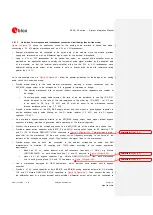
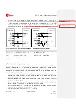
Figure 56: DDC (I
2
C) application circuit for u-blox 3.0 V GNSS receiver
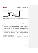
Reference
Description
Part Number – Manufacturer
R1, R2
4.7 k
Ω
Resistor 0402 5% 0.1 W
RC0402JR-074K7L - Yageo Phycomp
R3
47 k
Ω
Resistor 0402 5% 0.1 W
RC0402JR-0747KL - Yageo Phycomp
C2, C3
100 nF Capacitor Ceramic X5R 0402 10% 10V
GRM155R71C104KA01 - Murata
U1
Voltage Regulator for GNSS receiver
See GNSS receiver Hardware Integration Manual
U2
Generic Unidirectional Voltage Translator
SN74AVC2T245 - Texas Instruments
Table 32: Components for DDC (I
2
C) application circuit for u-blox 3.0 V GNSS receiver
ESD sensitivity rating of the DDC (I
2
C) pins is 1 kV (Human Body Model according to JESD22-
A114). Higher protection level could be required if the lines are externally accessible on the
application board. Higher protection level can be achieved by mounting an ESD protection (e.g.
EPCOS CA05P4S14THSG varistor array) close to accessible points.
2.5.3.2
Guidelines for DDC (I
2
C) layout design
The DDC (I
2
C) serial interface requires the same consideration regarding electro-magnetic interference as
any other digital interface. Keep the traces short and avoid coupling with RF line or sensitive analog
inputs, since the signals can cause the radiation of some harmonics of the digital data frequency.


