TOBY-L4 series - System Integration Manual
UBX-16024839 - R04
Design-in
Page 112 of 143
TOBY-L4 series
(Master, 1.8V)
BCLK
LRCLK
SDIN
SDOUT
GND
V_INT
I2Sx_CLK
I2Sx_WA
I2Sx_TXD
I2Sx_RXD
Audio Device
(Slave, 1.8V)
GND
TOBY-L4 series
(Slave, 1.8V)
BCLK
LRCLK
SDIN
SDOUT
GND
V_INT
I2Sx_CLK
I2Sx_WA
I2Sx_TXD
I2Sx_RXD
Audio Device
(Master, 1.8V)
GND
VDD
1V8
VDD
1V8
1V8
B1
A1
GND
U1
B3
A3
VCCB
VCCA
Unidirectional
Voltage Translator
C2
C1
3V0
DIR2
DIR3
OE
DIR1
B2
A2
B4
A4
DIR4
TOBY-L4 series
(Master, 1.8V)
BCLK
LRCLK
SDIN
SDOUT
GND
V_INT
I2Sx_CLK
I2Sx_WA
I2Sx_TXD
I2Sx_RXD
Audio Device
(Slave, 3.0V)
GND
VDD
TOBY-L4 series
(Slave, 1.8V)
BCLK
LRCLK
SDIN
SDOUT
GND
V_INT
I2Sx_CLK
I2Sx_WA
I2Sx_TXD
I2Sx_RXD
Audio Device
(Master, 3.0V)
GND
VDD
1V8
B1
A1
GND
U2
B3
A3
VCCB
VCCA
Unidirectional
Voltage Translator
C4
C3
3V0
DIR2
DIR4
OE
DIR3
B2
A2
B4
A4
DIR1
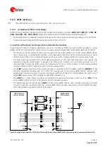
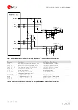
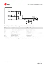
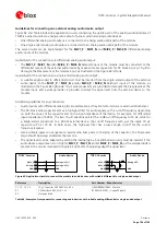
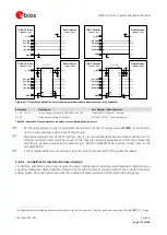
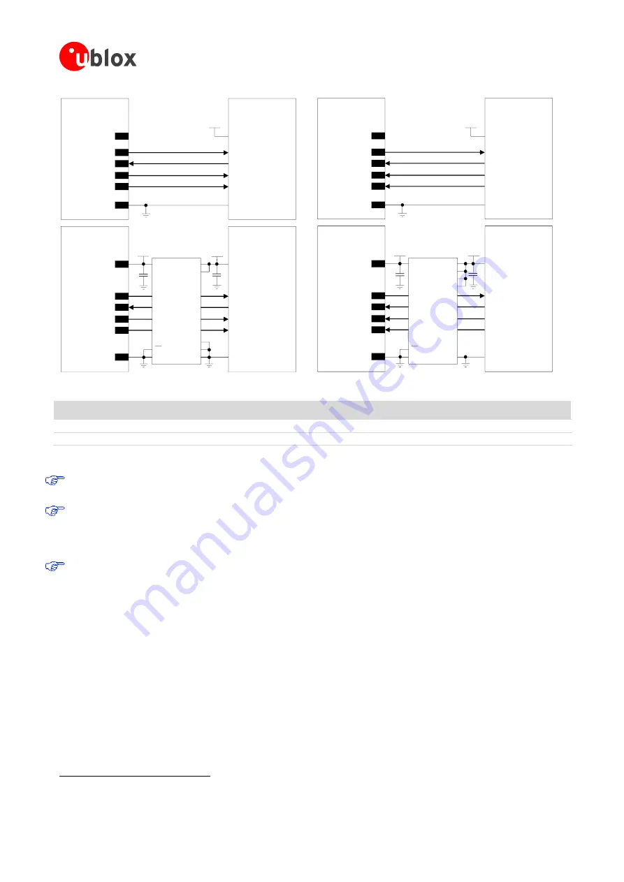
Figure 66: I
2
S interface application circuit with an external audio codec to provide voice capability
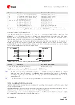
Reference
Description
Part Number – Manufacturer
C1, C2, C3, C4
100 nF Capacitor Ceramic X5R 0402 10% 10V
GRM155R71C104KA01 – Murata
U1, U2
Unidirectional Voltage Translator
SN74AVC4T774
20
- Texas Instruments
Table 50: Example of components for an audio voice codec application circuit
Do not apply voltage to any I
2
S pin before the switch-on of the I
2
S supply source (
V_INT
), to avoid latch-
up of circuits and allow a clean boot of the module.
The ESD sensitivity rating of the I
2
S interface pins is 1 kV (Human Body Model according to JESD22-A114).
A higher protection level could be required if the lines are externally accessible and it can be achieved by
mounting a general purpose ESD protection (e.g. EPCOS CA05P4S14THSG varistor array) close to the
accessible points.
If the I
2
S digital audio pins are not used, they can be left unconnected on the application board.
2.8.2.2
Guidelines for digital audio layout design
I
2
S interface and clock output lines require the same considerations regarding electromagnetic interference as
any other high speed digital interface. Keep the traces short and avoid coupling with RF lines / parts or sensitive
analog inputs, since the signals can cause the radiation of some harmonics of the digital data frequency.
20
Voltage translator providing partial power down feature so that the external 3 V supply can be also ramped up before
V_INT
1.8 V supply

