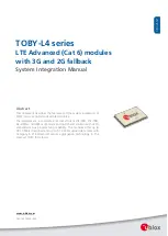
TOBY-L4 series - System Integration Manual
UBX-16024839 - R04
System description
Page 13 of 143
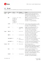
Function
Pin Name
Pin No
I/O
Description
Remarks
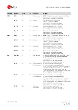
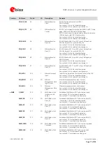
SIM0
VSIM
59
O
SIM0 supply output
VSIM
= 1.8 V / 3 V output as per the connected SIM type.
See section 1.8 for functional description.
See section 2.5 for external circuit design-in.
SIM_IO
57
I/O
SIM0 data
Data input/output for 1.8 V / 3 V SIM.
Internal 4.7 k
pull-up to
VSIM
.
See section 1.8 for functional description.
See section 2.5 for external circuit design-in.
SIM_CLK
56
O
SIM0 clock
3.9 MHz clock output for 1.8 V / 3 V SIM.
See section 1.8 for functional description.
See section 2.5 for external circuit design-in.
SIM_RST
58
O
SIM0 reset
Reset output for 1.8 V / 3 V SIM.
See section 1.8 for functional description.
See section 2.5 for external circuit design-in.
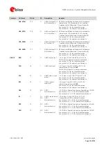
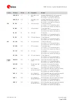
SIM1
VSIM1
172
O
SIM1 supply output
VSIM1
= 1.8 V / 3 V output as per the connected SIM type.
See section 1.8 for functional description.
See section 2.5 for external circuit design-in.
SIM1_IO
178
I/O
SIM1 data
Data input/output for 1.8 V / 3 V SIM.
Internal 4.7 k
pull-up to
VSIM1
.
See section 1.8 for functional description.
See section 2.5 for external circuit design-in.
SIM1_CLK
182
O
SIM1 clock
3.9 MHz clock output for 1.8 V / 3 V SIM.
See section 1.8 for functional description.
See section 2.5 for external circuit design-in.
SIM1_RST
177
O
SIM1 reset
Reset output for 1.8 V / 3 V SIM.
See section 1.8 for functional description.
See section 2.5 for external circuit design-in.
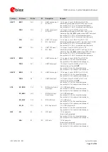
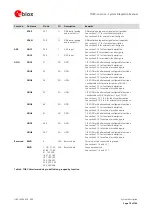
USB
VUSB_DET
4
I
USB detect input
VBUS (5 V typical) generated by the host must be connected
to this pin to enable the module USB device interface.
Test-Point for diagnostic / FW update access is
recommended.
See section 1.9.1 for functional description.
See section 2.6.1 for external circuit design-in.
USB_D–
27
I/O
USB High-Speed 2.0
diff. transceiver (–)
90
nominal differential impedance (Z
0
).
30
nominal common mode impedance (Z
CM
).
Pull-up or pull-down resistors and external series resistors as
required by the
USB 2.0 specifications
[3] are part of the
USB pin driver and need not be provided externally.
Test-Point for diagnostic / FW update access is recommended.
See section 1.9.1 for functional description.
See section 2.6.1 for external circuit design-in.
USB_D+
28
I/O
USB High-Speed 2.0
diff. transceiver (+)
90
nominal differential impedance (Z
0
).
30
nominal common mode impedance (Z
CM
).
Pull-up or pull-down resistors and external series resistors as
required by the
USB 2.0 specifications
[3] are part of the
USB pin driver and need not be provided externally.
Test-Point for diagnostic / FW update access is recommended.
See section 1.9.1 for functional description.
See section 2.6.1 for external circuit design-in.
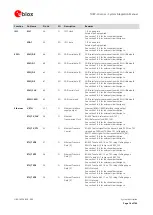
USB_ID
168
I
USB device
identification
Pin for ID resistance measurement.
See section 1.9.1 for functional description.
See section 2.6.1 for external circuit design-in.

