TOBY-L4 series - System Integration Manual
UBX-16024839 - R04
System description
Page 28 of 143
1.5.1.5
VCC current consumption in cyclic idle/active mode (power saving enabled)
The power saving configuration is disabled by default, but it can be enabled using the AT+UPSV command (see
the
u-blox AT Commands Manual
[2]) or the dedicated uCPU API. When power saving is enabled, the module
automatically enters the low power idle mode whenever possible, reducing current consumption.
During low power idle mode, the module processor runs with 32 kHz reference clock frequency.
When the power saving configuration is enabled and the module is registered or attached to a network, the
module automatically enters the low power idle mode whenever possible, but it must periodically monitor the
paging channel of the current base station (paging block reception), in accordance with the 2G/3G/LTE system
requirements, even if connected mode is not enabled by the application. When the module monitors the paging
channel, it wakes up to the active mode to enable the reception of the paging block. In between, the module
switches to low power idle mode. This is known as discontinuous reception (DRX).
The module processor core is activated during the paging block reception, and automatically switches its
reference clock frequency from 32 kHz to the 26 MHz used in active mode.
The time period between two paging block receptions is defined by the network. This is the paging period
parameter, fixed by the base station through the broadcast channel sent to all users on the same serving cell:
For 2G radio access technology, the paging period can vary from 470.8 ms (DRX = 2, length of 2 x 51 2G
frames = 2 x 51 x 4.615 ms) up to 2118.4 ms (DRX = 9, length of 9 x 51 2G frames = 9 x 51 x 4.615 ms)
For 3G radio access technology, the paging period can vary from 640 ms (DRX = 6, i.e. length of 2
6
3G
frames = 64 x 10 ms) up to 5120 ms (DRX = 9, length of 2
9
3G frames = 512 x 10 ms).
For LTE radio access technology, the paging period can vary from 320 ms (DRX = 5, i.e. length of 2
5
LTE
frames = 32 x 10 ms) up to 2560 ms (DRX = 8, length of 2
8
LTE frames = 256 x 10 ms).
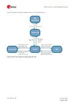
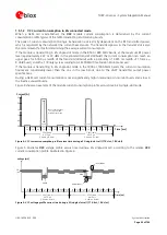
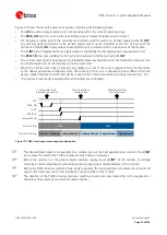
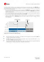
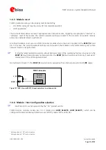
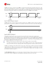
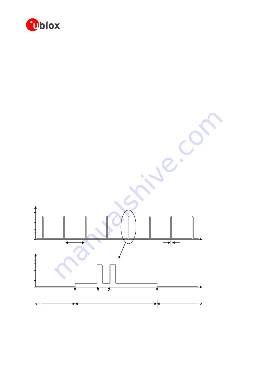
Figure 9 illustrates a typical example of the module current consumption profile when power saving is enabled.
The module is registered with the network, automatically enters the low power idle mode and periodically wakes
up to active mode to monitor the paging channel for the paging block reception.
~50 ms
IDLE MODE
ACTIVE MODE
IDLE MODE
Active Mode
Enabled
Idle Mode
Enabled
2G case: 0.44-2.09 s
3G case: 0.61-5.09 s
LTE case: 0.27-2.51 s
IDLE MODE
~50 ms
ACTIVE MODE
Time [s]
Current [mA]
Time [ms]
Current [mA]
RX
Enabled
0
100
0
100
Figure 9: VCC current consumption profile with power saving enabled and module registered with the network: the module is
in low-power idle mode and periodically wakes up to active mode to monitor the paging channel for paging block reception

