TOBY-L4 series - System Integration Manual
UBX-16024839 - R04
System description
Page 34 of 143
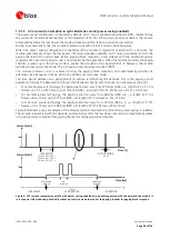
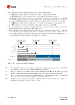
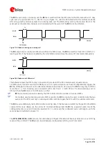
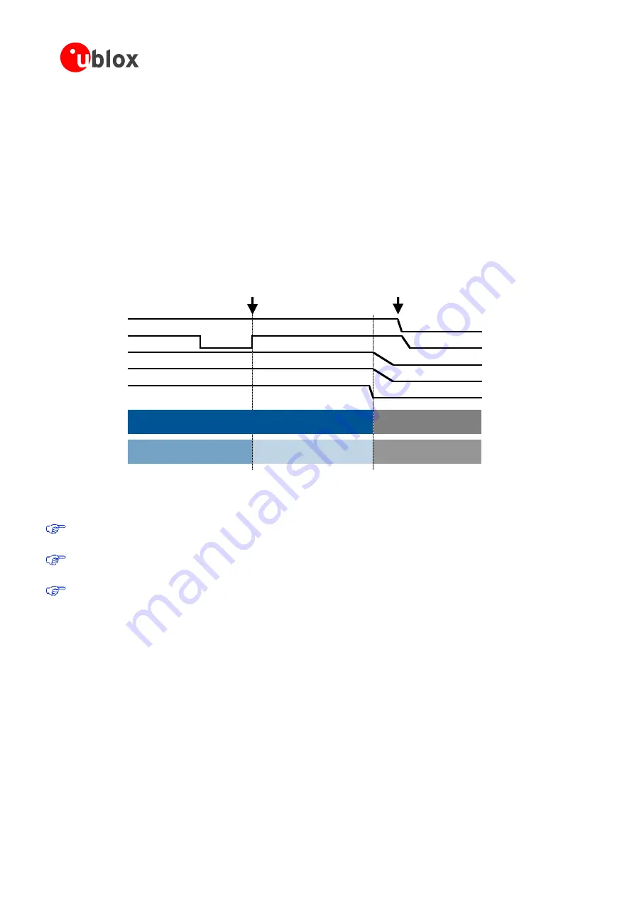
Figure 14 describes the TOBY-L4 series modules’ switch-off sequence started by means of the
PWR_ON
input
pin, allowing storage of current parameter settings in the module’s non-volatile memory and a clean network
detach, with the following phases
A low pulse with the appropriate time duration is applied at the
PWR_ON
input pin, which is normally set
high by an internal pull-up: the module starts the switch-off routine when the
PWR_ON
signal is released
from the low logical level.
At the end of the switch-off routine, all the digital pins are tri-stated and all the internal voltage regulators
are turned off, including the generic digital interfaces supply (
V_INT
).
Then, the module remains in power-off mode as long as a switch-on event does not occur (i.e. applying a
suitable low level pulse to the
PWR_ON
input pin), and enters not-powered mode if the supply is removed
from the
VCC
pins.
VCC
PWR_ON
RESET_N
V_INT
Internal Reset
System State
BB Pads State
OFF
Tristate / Floating
ON
Operational
->
Tristate
Operational
0 s
~2.5 s
~5 s
The module starts
the switch-off routine
VCC
can be removed
Figure 14: TOBY-L4 series power-off sequence description
The Internal Reset signal is not available on a module pin, but the application can monitor the
V_INT
pin
to sense the end of the power-off sequence.
The
VCC
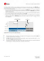
supply can be removed only after the end of the module internal switch-off routine, i.e. only
after that the
V_INT
voltage level has gone low.
The duration of each phase in the TOBY-L4 series modules’ switch-off routines can largely vary depending
on the application / network settings and the concurrent module activities.

