TOBY-L4 series - System Integration Manual
UBX-16024839 - R04
Design-in
Page 99 of 143
Reference
Description
Part Number - Manufacturer
C1, C2
1 µF Capacitor Ceramic X7R 0603 10% 25 V
GRM188R71E105KA12 - Murata
C3, C4
10 nF Capacitor Ceramic X7R 0402 10% 16 V
GRM155R71C103KA01 - Murata
C5, C6
10 µF Capacitor Ceramic X5R 0603 20% 6.3 V
GRM188R60J106ME47 - Murata
R1
470 k
Resistor 0402 5% 0.1 W
RK73B1ETTD474J - KOA
R2, R3, R4, R5, R6, R7 22
Resistor 0402 5% 0.1 W
RK73B1ETTP220J - KOA
R8
47 k
Resistor 0402 5% 0.1 W
RK73B1ETTD473J - KOA
R9
47 k
Resistor 0402 5% 0.1 W
RK73B1ETTD473J - KOA
U1
LDO Linear Regulator 3.3 V 0.5 A
LT1963CS8-3.3 - Linear Technology
U2
LDO Linear Regulator 1.8 V 0.3 A
LT1962EMS8-1.8 - Linear Technology
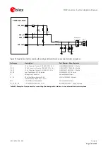
Table 42: Components for connecting TOBY-L4 cellular modules and u-blox EMMY-W161 short range communication modules
Connection with external SDIO devices
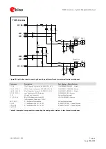
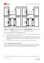
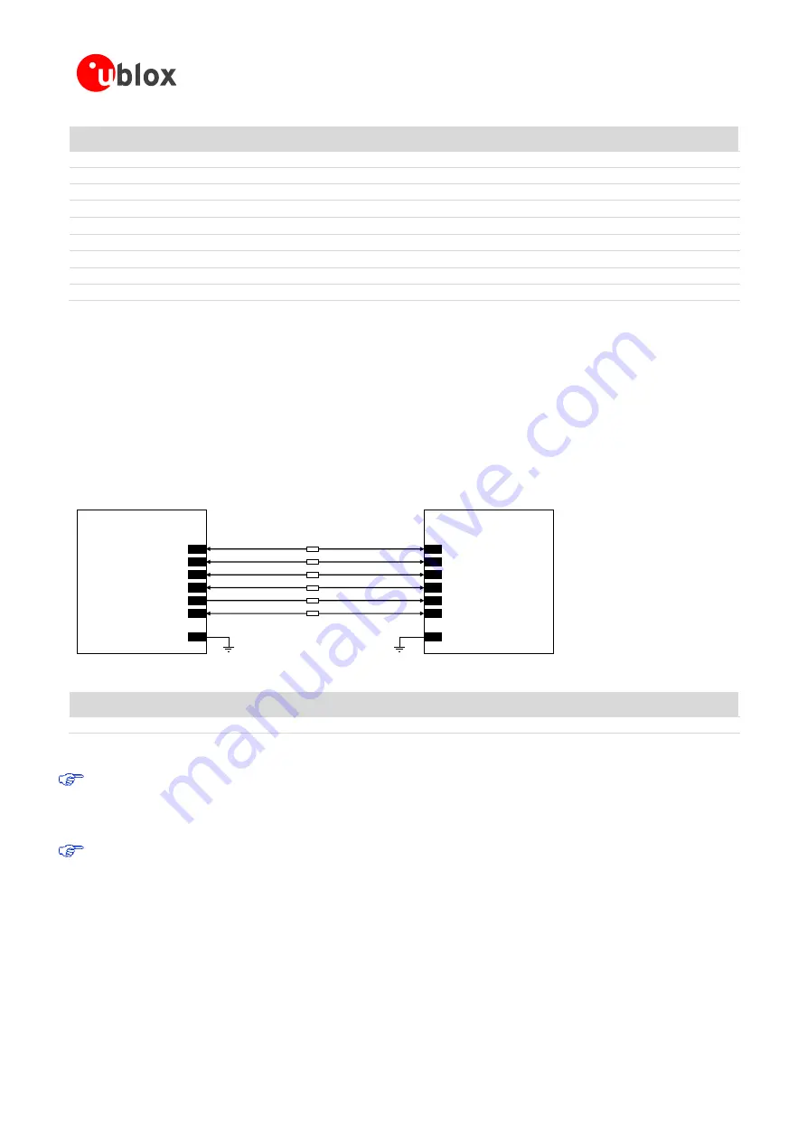
Figure 58 and Table 43 show an application circuit example for connecting the SDIO interface of TOBY-L4 series
modules to a 1.8 V SDIO device: the SDIO pins of the cellular module are connected to the related SDIO pins of
the SDIO device, with appropriate low value series damping resistors to avoid reflections and other losses in
signal integrity, which may create ringing and loss of a square wave shape.
The most appropriate value for the series damping resistors on the SDIO lines depends on the specific line
lengths and layout implemented. In general, the SDIO series resistors are not strictly required, but it is
recommended to slow the SDIO signal, for example with 22
or 33
resistors, and avoid any possible ringing
problem without violating the rise / fall time requirements.
R2
SDIO Device
SD_D0
SD_D1
SD_D2
SD_D3
SD_CLK
SD_CMD
TOBY-L4 series
SDIO_D0
66
SDIO_D1
68
SDIO_D2
63
SDIO_D3
67
SDIO_CLK
64
SDIO_CMD
65
R3
R4
R5
R6
GND
GND
R1
Figure 58: Application circuit for connecting TOBY-L4 series modules to a 1.8 V SDIO device
Reference
Description
Part Number - Manufacturer
R1, R2, R3, R4, R5, R6 22
Resistor 0402 5% 0.1 W
RK73B1ETTP220J - KOA
Table 43: Components for connecting TOBY-L4 series modules to a 1.8 V SDIO device
The ESD sensitivity rating of SDIO interface pins is 1 kV (HMB according to JESD22-A114). A higher
protection level could be required if the lines are externally accessible and this can be achieved by
mounting a very low capacitance ESD protection (e.g. Tyco Electronics PESD0402-140 ESD) close to the
accessible points.
If the SDIO interface pins are not used, they can be left unconnected on the application board.
2.6.5.2
Guidelines for SDIO layout design
The SDIO serial interface requires the same considerations regarding electro-magnetic interference as any other
high speed digital interface.
Keep the traces short, avoid stubs and avoid coupling with RF lines / parts or sensitive analog inputs, since the
signals can cause the radiation of some harmonics of the digital data frequency.
Consider the usage of low value series damping resistors to avoid reflections and other losses in signal integrity,
which may create ringing and loss of a square wave shape.

