

TOBY-L4 series - System Integration Manual
UBX-16024839 - R04
Handling and soldering
Page 121 of 143
3.3
Soldering
3.3.1
Soldering paste
"No Clean" soldering paste is strongly recommended for TOBY-L4 series modules, as it does not require cleaning
after the soldering process has taken place. The paste listed in the example below meets these criteria.
Soldering Paste:
OM338 SAC405 / Nr.143714 (Cookson Electronics)
Alloy specification:
95.5% Sn / 3.9% Ag / 0.6% Cu (95.5% Tin / 3.9% Silver / 0.6% Copper)
95.5% Sn / 4.0% Ag / 0.5% Cu (95.5% Tin / 4.0% Silver / 0.5% Copper)
Melting Temperature: +217 °C
Stencil Thickness:
150 µm for base boards
The final choice of the soldering paste depends on the approved manufacturing procedures.
The paste-mask geometry for applying soldering paste should meet the recommendations in section 2.13.
The quality of the solder joints on the connectors (“half vias”) should meet the appropriate IPC
specification.
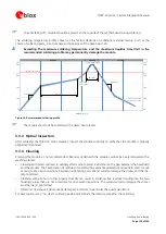
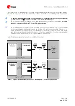
3.3.2
Reflow soldering
A convection type-soldering oven is strongly recommended
for TOBY-L4 series modules over the infrared
type radiation oven. Convection heated ovens allow precise control of the temperature and all parts will be
heated up evenly, regardless of material properties, thickness of components and surface color.
Refer to the ”IPC-7530 Guidelines for temperature profiling for mass soldering (reflow and wave) processes”
guide, published in 2001.
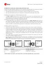
Reflow profiles are to be selected according to the following recommendations.
Failure to observe these recommendations can result in severe damage to the device!
Preheat phase
Initial heating of component leads and balls. Residual humidity will be dried out. Note that this preheat phase
will not replace prior baking procedures.
Temperature rise rate: max 3 °C/s
If the temperature rise is too rapid in the preheat phase, it may cause
excessive slumping.
Time: 60 – 120 s
If the preheat is insufficient, rather large solder balls tend to be
generated. Conversely, if performed excessively, fine balls and large
balls will be generated in clusters.
End Temperature: 150 °C - 200 °C
If the temperature is too low, non-melting tends to be caused in
areas containing large heat capacity.
Heating/ reflow phase
The temperature rises above the liquidus temperature of +217 °C. Avoid a sudden rise in temperature as the
slump of the paste could become worse.
Limit time above +217 °C liquidus temperature: 40 - 60 s
Peak reflow temperature: +245 °C
Cooling phase
A controlled cooling avoids negative metallurgical effects (solder becomes more brittle) of the solder and
possible mechanical tensions in the products. Controlled cooling helps to achieve bright solder fillets with a good
shape and low contact angle.
Temperature fall rate: max 4 °C/s


