TOBY-L4 series - System Integration Manual
UBX-16024839 - R04
Design-in
Page 60 of 143
2.2.1.6
Additional guidelines for VCC supply circuit design
To reduce voltage drops, use a low impedance power source. The series resistance of the power supply lines
(connected to the modules’
VCC
and
GND
pins) on the application board and battery pack should also be
considered and minimized: cabling and routing must be as short as possible to minimize power losses.
Three pins are allocated to the
VCC
supply. Several pins are designated for
GND
connection. It is recommended
to correctly connect all of them to supply the module to minimize series resistance losses.
For modules supporting 2G radio access technology, to avoid voltage drop undershoot and overshoot at the
start and end of a transmit burst during a GSM call (when current consumption on the
VCC
supply can rise up as
specified in the
TOBY-L4 series
Data Sheet
[1]), place a bypass capacitor with large capacitance (at least 100 µF)
and low ESR near the
VCC
pins, for example:
330 µF capacitance, 45 m
ESR (e.g. KEMET T520D337M006ATE045, Tantalum Capacitor)
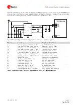
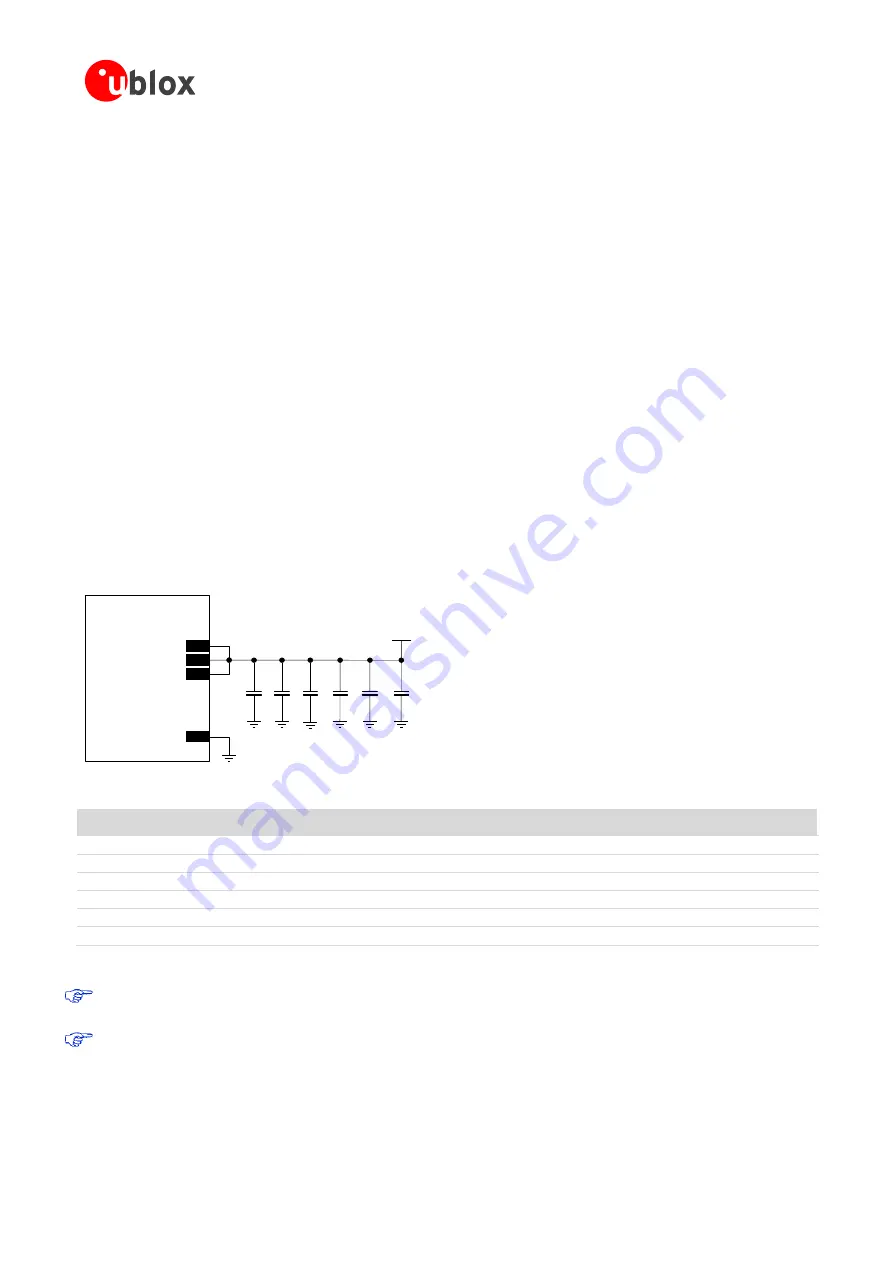
To reduce voltage ripple and noise, improving RF performance especially if the application device integrates an
internal antenna, place the following bypass capacitors near the
VCC
pins:
68 pF capacitor with Self-Resonant Frequency in the 800/900 MHz range (e.g. Murata GRM1555C1H680J)
15 pF capacitor with Self-Resonant Frequency in 1800/1900 MHz range (e.g. Murata GRM1555C1E150J)
8.2 pF capacitor with Self-Resonant Frequency in 2500/2600 MHz range (e.g. Murata GRM1555C1H8R2D)
10 nF capacitor (e.g. Murata GRM155R71C103K) to filter digital logic noise from clocks and data sources
100 nF capacitor (e.g. Murata GRM155R61C104K) to filter digital logic noise from clocks and data sources
A suitable series ferrite bead can be correctly placed on the
VCC
line for additional noise filtering if required by
the specific application according to the whole application board design.
C2
GND
C3
C4
TOBY-L4 series
71
VCC
72
VCC
70
VCC
C1
C5
C6
3V8
+
Figure 24: Suggested schematic for the VCC bypass capacitors to reduce ripple / noise on the supply voltage profile
Reference
Description
Part Number - Manufacturer
C1
8.2 pF Capacitor Ceramic C0G 0402 5% 50 V
GRM1555C1H8R2DZ01 - Murata
C2
15 pF Capacitor Ceramic C0G 0402 5% 50 V
GRM1555C1H150JA01 - Murata
C3
68 pF Capacitor Ceramic C0G 0402 5% 50 V
GRM1555C1H680JA01 - Murata
C4
10 nF Capacitor Ceramic X7R 0402 10% 16 V
GRM155R71C103KA01 - Murata
C5
100 nF Capacitor Ceramic X7R 0402 10% 16 V
GRM155R71C104KA01 - Murata
C6
330 µF Capacitor Tantalum D_SIZE 6.3 V 45 m
T520D337M006ATE045 - KEMET
Table 17: Suggested components to reduce ripple / noise on the VCC
The necessity of each part depends on the specific design, but it is recommended to provide all the bypass
capacitors illustrated in Figure 24 / Table 17 if the application device integrates an internal antenna.
The ESD sensitivity rating of the
VCC
supply pins is 1 kV (HBM as per JESD22-A114). A higher protection
level can be required if the line is externally accessible on the application board, e.g. if the accessible
battery connector is directly connected to the supply pins. A higher protection level can be achieved by
mounting an ESD protection (e.g. EPCOS CA05P4S14THSG varistor) close to the accessible point.

