background image


12


Customizing the CC1 

4.1 Overview 

The CC1 is an open-source platform that was developed to give as much flexibility to users as 
possible. This means that the internal firmware that operates the device can be changed by the 
user, if desired. Inside the CC1, two programmable electronic components are responsible for 
most of the functionality of the CC1. They include: 

  A Rabbit RCM3400 Microprocessor 

  An Altera Cyclone IV FPGA 

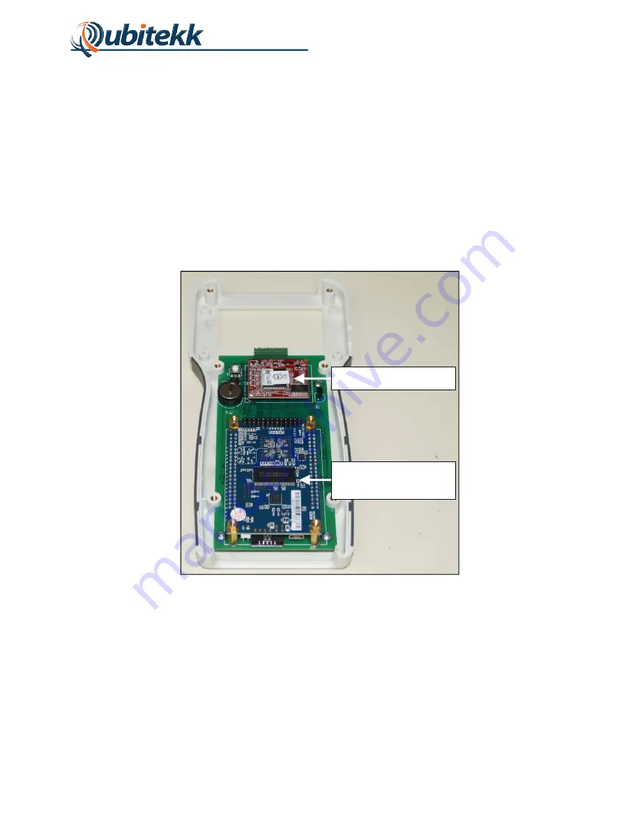
The location of these components inside the CC1 is shown below: 


Figure 9. Internal view of CC1 electronics. 

The RCM3400 microprocessor is used to implement the user interface (i.e. LCD display, menus, 
serial communicatons, etc.) as well as some very simple calculations (i.e. accidentals). The 
Altera FPGA is used for making high speed measurements (i.e. the coincidence counting). 

These two devices can be independently programmed to realize new functionality for a wide 
range of applications. For example, the CC1 device could be reprogrammed to timestamp every 
photon detection event and create a histogram of the arrival times. Or two CC1s could be re-
programmed to act as a four photon coincidence counter (using the GATE channel as a 

Rabbit


RCM3400


module


Altera


Cyclone


IV


FPGA


(on


DE0

Nano


protoboard)


Summary of Contents for CC1

Page 1: ...CC1 Handheld Coincidence Counter USER S MANUAL Rev 1 02 June 1 2015 www qubitekk com...

Page 2: ...2 3 Dwell Time 8 2 4 Gate Chan 8 2 5 Subtract Acc 8 2 6 Trigger 9 2 7 CH1 Delay 9 2 8 Firmware 9 3 Serial Interface 10 3 1 Serial Interface Setup 10 3 2 Programming Commands 10 3 3 Sample Code 11 4 C...

Page 3: ...4 2 3 Programming the Cyclone IV FPGA 18 Appendix A Electrical Schematics and Connections 20 A 1 Top Board LCD Board 21 A 2 Bottom Board Processor Board 22 A 3 Pinout Table 25...

Page 4: ...with all of the functionality described in this manual however it is capable of much more The unit contains both a re programmable microprocessor for handling the user interface and serial communicati...

Page 5: ...d through its USB port The USB cable provided with the system should be plugged into the side of the unit as shown in Figure 2 Figure 2 Power over USB connection The other end of the USB cable can be...

Page 6: ...connector jacks are available at the top of the unit To detect coincident pulses Channels 1 and 2 must both be connected to a pulse signal If the counting of single and coincidence pulses should be ga...

Page 7: ...4 Figure 4 CC1 Buttons and Ports...

Page 8: ...for modification by pressing the ENABLE button The setting value will blink indicating that it is ready for modification Again the UP and DOWN arrow buttons can be pressed to change the setting value...

Page 9: ...FF button has been pressed the details of the count measurement will be displayed on the LCD as shown in Figure 6 Figure 6 Count Screen after measurement Once the measurement is complete the counts wi...

Page 10: ...will be counted by the CC1 to be coincident if a The time between the rising edges of the two pulses is less than the coincidence window If the GATE signal is enabled then the two pulses will only be...

Page 11: ...s initiated the CC1 will accumulate counts for an amount of time equal to the Dwell Time If the Dwell Time is infinity the CC1 will accumulate counts indefinitely or until the ON OFF button is pressed...

Page 12: ...of time Then the unit s counters will automatically be reset and a new count initiated This cycle will continue over and over until the ON OFF button is again pressed to halt continuous triggering If...

Page 13: ...command is not recognized the CC1 will reply with Unknown Command Command Description COUN C1 C2 CO Returns the current value on the counter either Channel 1 C1 Channel 2 C2 or Coincidences CO CLEA S...

Page 14: ...3 Output DWEL 20000 Chr 13 Set Dwell Time to 20 seconds Sleep 300 Wait 0 3 seconds for command to transfer MSComm3 Output DELA 2 Chr 13 Set Delay Time on Channel 1 to 2ns Sleep 300 Wait 0 3 seconds fo...

Page 15: ...iew of CC1 electronics The RCM3400 microprocessor is used to implement the user interface i e LCD display menus serial communicatons etc as well as some very simple calculations i e accidentals The Al...

Page 16: ...h your unit Rabbit Programming Cable 2mm A great resource for learning Dynamic C and how to program the RCM3400 is the book entitled Embedded Systems Design using the Rabbit 3000 Microprocessor by Kam...

Page 17: ...bitekk website frequently for the latest versions of the default firmware 4 2 Uploading Custom Firmware 4 2 1 Accessing the Programming Ports To upload new firmware to your CC1 it is necessary to firs...

Page 18: ...in Figure 12 Figure 12 Programming ports exposed 4 2 2 Programming the Rabbit RCM3400 To program the Rabbit RCM3400 a bin programming file must first be created in the Dynamic C 9 62 development envi...

Page 19: ...to the Rabbit Programming Port on the base of your CC1 unit as shown in Figure 14 note orientation of red wire Figure 14 Creating a programming file for the RCM3400 With the Rabbit Programming Cable i...

Page 20: ...not be recognized automatically If this happens you will get an error that says Could not open serial port If this occurs you will need to select the Setup Communications item in the DC RFU program me...

Page 21: ...nu item File Convert Programming Files in Quartus II This will open the Convert Programming File window which allows various parameters to be provided by the user to convert a sof file to a jic file I...

Page 22: ...programming Select the Tools Programmer menu option in Quartus II to open the Altera Programmer window Click the Add File button to add the jic file that was just created and select the USB Blaster b...

Page 23: ...20 APPENDIX A Electrical Schematics and Connections...

Page 24: ...21 A 1 Top Board LCD Display...

Page 25: ...22 A 2 Bottom Board FPGA and Microprocessor...

Page 26: ...23...

Page 27: ...24...

Page 28: ...Display Line 4 20 PE2 Clear Button on User Interface 21 PE1 Bus to LCD Display Line 5 22 PE0 Menu Button on User Interface 23 GND Ground 24 3_3V_IN 3 3V Input Power 25 PG7 Bus to LCD Display Line 6 2...

Page 29: ...to FPGA Counter Bit 10 30 PD5 Enable GATE Signal Flag for FPGA 31 PD6 Bus to FPGA Counter Bit 11 32 RESET_IN Reserved for firmware upload 33 PD7 Bus to FPGA Counter Bit 12 34 VBAT_EXT Reserved for Ba...

Page 30: ...tput to RCM3400 Bit 6 38 IO31 FPGA Counter Output to RCM3400 Bit 11 39 IO32 FPGA Counter Output to RCM3400 Bit 7 40 IO33 FPGA Counter Output to RCM3400 Bit 12 JP2 1 IN0 Not Connected 2 IO00 Not Connec...

Page 31: ...GND2 Ground 31 IO24 Not Connected 32 IO25 Not Connected 33 IO26 Not Connected 34 IO27 Not Connected 35 IO28 Not Connected 36 IO29 Not Connected 37 IO30 Not Connected 38 IO31 Not Connected 39 IO32 Not...

Reviews: