EVK-NINA-B4 - User guide
UBX-19054587 - R04
Interfaces and peripherals
Page 25 of 40
C1 - Public
5.2
Arduino interface
The EVK-NINA-B4 includes a set of pin headers and mounting holes that are compatible with certain
Arduino or Arduino inspired shields.
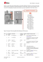
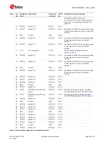
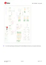
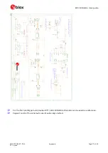
Figure 16 shows the layout of the Arduino interface described in Table 12. See also
Arduino shield
compatibility
for information about compatible shields for EVK-NINA-B4.
Figure 16: Pin headers that are compatible with some Arduino shields
Conn.
Pin
No.
Arduino
pin
Description
Schematic
net name
nRF52
pin
Alternate functions and notes
J1
1
N/C
Not Connected
-
-
Not connected
2
IOREF
I/O reference voltage level.
Selectable by user to 1.7
–
3.6 V
VDD_IO
-
See also
Selecting the power
configuration jumpers
3
RESET
NINA reset signal input. Active low
logic
RESET_N
P0.18
4
3.3V
3.3 V DC regulated supply output
3V3
-
5
5V
5 V regulated supply output
5V
-
Cannot be used as supply input, use
VIN instead. Only supplied by USB
VBUS.
6
GND
Ground
GND
GND
7
GND
Ground
GND
GND
8
VIN
External DC supply input, 5
–
12 VDC VIN
-
J1
J2
J3
J4
Mounting Holes
Arduino Interface
J1
1
8
N/C
VDD_IO
RESET_N
3V3
5 V
GND
GND
VIN
J2
1
6
A0/GPIO_25
A1/GPIO_24
A2/GPIO_27
A3/GPIO_18
A4/GPIO_17
A5/GPIO_16
J3
1
8
D5/GPIO_32
D4/GPIO_1
D3/GPIO_20
D2/GPIO_21
TX/D1/GPIO_22
RX/D0/GPIO_23
D6/GPIO_28
D7/GPIO_29
J4
1
10
SCL/GPIO_5
SDA/GPIO_4
N/C
GND
D13/GPIO_45
D12/GPIO_8
(D11/GPIO_3)
(D10/GPIO_2)
D9/GPIO_46
D8/GPIO_33


