EVK-NINA-B4 - User guide
UBX-19054587 - R04
Product description
Page 9 of 40
C1 - Public
2.5
Connectors
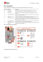
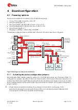
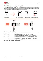
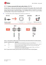
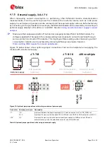
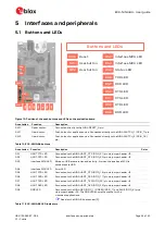
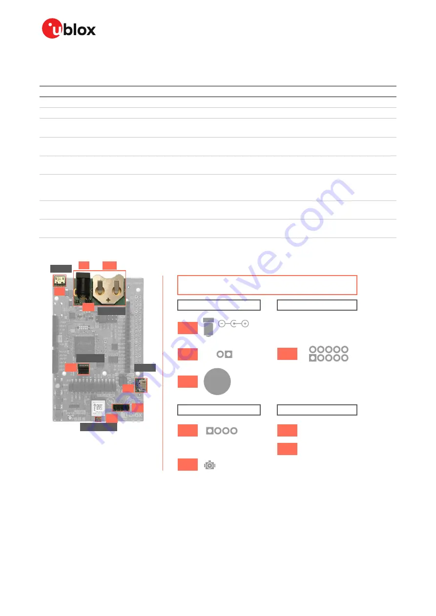
Table 1 describes the available connectors of the EVK-NINA-B4 shown in Figure 4.
Connector Function
Description
J5
Power supply
2.1 mm power jack, the center pin is the positive terminal. 5
–
12 V input.
J17
Power supply
Pin header that can be used to connect external power supplies. 5
–
12 V input.
BT1
Battery holder
CR2032 coin cell battery holder. CR2032 usually has a 3 V potential when fully
charged.
J11
NFC antenna connector Pin header that connects to the u-blox NFC antenna included in the kit. The antenna
can be mounted in either direction.
(J2)
2.4 GHz RF antenna
connector
U.FL coaxial connector that can be used to connect antennas or RF equipment. This
connector is only included in the EVK-NINA-B400/EVK-NINA-B410.
J12
Cortex Debug connector 10-pin, 50 mil pitch connector that can be used to connect external debuggers to the
NINA-B4 module. The NINA-B4 modules support Serial Wire debug (SWD) and Serial
Wire Viewer, but not JTAG debug.
J8
Power supply, COM port
and debug USB
The main USB connector that is used to program, debug, and communicate with the
NINA module. It can also be used to power the entire board.
J16
Power supply and NINA
USB port
Additional USB connector directly connected to the NINA-B4 USB interface. Can also
be used to power the entire board.
Table 1: EVK-NINA-B4 connector description
Figure 4: Available connectors and their pinout
J5
2 1
1
4
GND
VIN
5 - 12 V
NF
C1
GND
GND
NF
C2
U.FL RF coax, (J2 is the module designator)
GND
GND
N/
C
VDD
_IO
GND
S
WDIO
S
WD
CL
K
GP
IO
_8
N/
C
RE
SET
_N
BT1
J17
Power
J8
J16
USB
Debug
J12
Antennas
J11
(J2)
CR2032
+
3V
2
1
10
9
Micro USB
Micro USB
J17
Debug
Power
Antennas
USB
USB
J8
J5
BT1
J12
J16
(J2)
J11
Board Connectors

