


MAX-M5Q - Hardware Integration Manual
FTX-HW-13008
Objective Specification
Product handling
Page 28 of 40
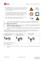
6
Product handling
6.1
Packaging, shipping, storage and moisture preconditioning
For information pertaining to reels and tapes, Moisture Sensitivity levels (MSD), shipment and storage
information, as well as drying for preconditioning see MAX-M5Q Data Sheet, Docu. No FTX-HW-13003 [1].
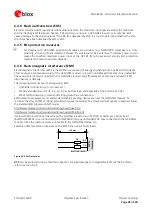
6.1.1
Population of Modules
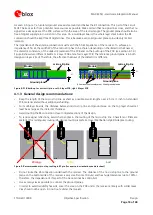
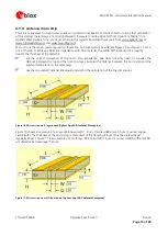
When populating our modules make sure that the pick and place machine is aligned to the copper pins
of the module and not on the module edge.
6.2
Soldering
6.2.1
Soldering paste
Use of "No Clean" soldering paste is strongly recommended, as it does not require cleaning after the soldering
process has taken place. The paste listed in the example below meets these criteria.
Soldering Paste:
OM338 SAC405 / Nr.143714 (Cookson Electronics)
Alloy specification:
Sn 95.5/ Ag 4/ Cu 0.5 (95.5% Tin/ 4% Silver/ 0.5% Copper)
Melting Temperature: 217 °C
Stencil Thickness:
see section 3.3.1
The final choice of the soldering paste depends on the approved manufacturing procedures.
The paste-mask geometry for applying soldering paste should meet the recommendations.
The quality of the solder joints on the connectors (’half vias’) should meet the appropriate IPC
specification.
6.2.2
Reflow soldering
A convection type-soldering oven is strongly recommended
over the infrared type radiation oven.
Convection heated ovens allow precise control of the temperature and all parts will be heated up evenly,
regardless of material properties, thickness of components and surface color.
Consider the "IPC-7530 Guidelines for temperature profiling for mass soldering (reflow and wave) processes,
published 2001. “
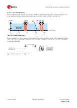
Preheat phase
Initial heating of component leads and balls. Residual humidity will be dried out. Please note that this preheat
phase will not replace prior baking procedures.
•
Temperature rise rate: max. 3 °C/s
If the temperature rise is too rapid in the preheat phase it may cause
excessive slumping.
•
Time: 60 - 120 s
if the preheat is insufficient, rather large solder balls tend to be generated. Conversely,
if performed excessively, fine balls and large balls will be generated in clusters.
•
End Temperature: 150 - 200 °C
If the temperature is too low, non-melting tends to be caused in areas
containing large heat capacity.
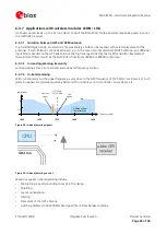
Heating/ Reflow phase
The temperature rises above the liquidus temperature of 217°C. Avoid a sudden rise in temperature as the slump
of the paste could become worse.
•
Limit time above 217 °C liquidus temperature: 40 - 60 s
•
Peak reflow temperature: 245 °C


