background image

MAX-M5Q - Hardware Integration Manual 

FTX-HW-13008 

Objective Specification 

Product handling 


Page 33 of 40


6.3.4


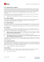
Electrical Overstress (EOS) 

Electrical Overstress (EOS) usually describes situations when the maximum input power exceeds the maximum 
specified ratings. EOS failure can happen if RF emitters are close to a GPS/GNSS receiver or its antenna. EOS 
causes damage to the chip structures. If the RF_IN is damaged by EOS, it is hard to determine whether the chip 
structures have been damaged by ESD or EOS. 

6.3.5


EOS protection measures 


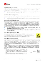
For designs with GPS/GNSS positioning modules and wireless (e.g. GSM/GPRS) transceivers in close 
proximity, ensure sufficient isolation between the wireless and GPS antennas. If wireless power output 
causes the specified maximum power input at the GPS RF_IN to be exceeded, employ EOS protection 
measures to prevent overstress damage.  

6.3.6


Electromagnetic interference (EMI) 

Electromagnetic interference (EMI) is the addition or coupling of energy originating from any RF emitting device. 
This can cause a spontaneous reset of the GPS/GNSS receiver or result in unstable performance. Any unshielded 
line or segment (>3mm) connected to the GPS/GNSS receiver can effectively act as antenna and lead to EMI 
disturbances or damage. 
The following elements are critical regarding EMI: 


Unshielded connectors (e.g. pin rows etc.) 


Weakly shielded lines on PCB (e.g. on top or bottom layer and especially at the border of a PCB) 


Weak GND concept (e.g. small and/or long ground line connections)  

EMI protection measures are recommended when RF emitting devices are near the GPS/GNSS receiver. To 
minimize the effect of EMI a robust grounding concept is essential. To achieve electromagnetic robustness follow 
the standard EMI suppression techniques. 
http://www.murata.com/products/emc/knowhow/index.html 
http://www.murata.com/products/emc/knowhow/pdf/4to5e.pdf 
Improved EMI protection can be achieved by inserting a resistor (e.g. R>20 

) or better yet a ferrite bead 

(BLM15HD102SN1) or an inductor (LQG15HS47NJ02) into any unshielded PCB lines connected to the GPS/GNSS 
receiver. Place the resistor as close as possible to the GPS/GNSS receiver pin.  
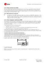
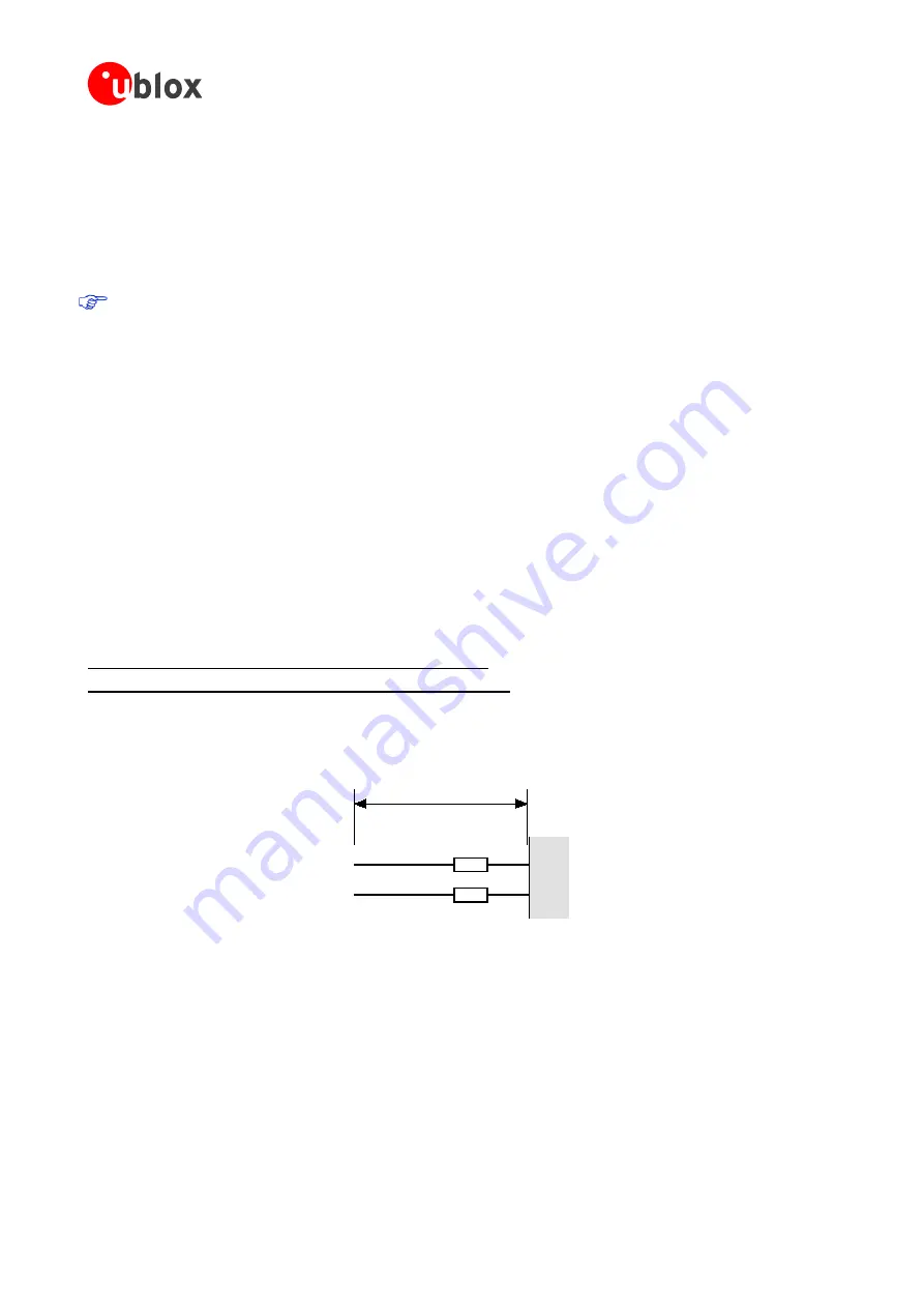
Example of EMI protection measures on the RX/TX line using a ferrite bead: 

TX

RX

G

P

S

R

ec

ei

ver

FB

FB

BLM15HD102SN1

>10mm


Figure 22: EMI Precautions 

VCC

 can be protected using a feed thru capacitor. For electromagnetic compatibility (EMC) of the RF_IN pin, 

refer to section 6.3.5 
 

Summary of Contents for MAX-M5Q

Page 1: ...he features and specifications of the MAX M5Q in MAX form factor with Mediatek hybrid parallel GPS GGLONASS receiver This stand alone module is compact and easy to integrate and provides an easy upgra...

Page 2: ...pecification This document applies to the following products Name Type number ROM FLASH version PCN reference MAX M5Q 0 All Flash FW320G UBX 3135 This document and the use of any information contained...

Page 3: ...nstructions and information on how to set up production and final product tests Application Notes These documents provide general design instructions and information that applies to all u blox GPS GNS...

Page 4: ...es by email Use our service pool email addresses rather than any personal email address of our staff This ensures that we process your request as soon as possible You will find the contact details at...

Page 5: ...VCC Main Supply Voltage 11 2 5 2 V_BCKP Backup Supply Voltage 11 2 5 3 VCC_IO 11 2 5 4 VCC_RF Output Voltage RF section 11 2 6 Interfaces 12 2 6 1 UART 12 2 7 I O pins 12 2 7 1 Antenna input 12 2 7 2...

Page 6: ...ns to a MAX 8x module 27 5 2 1 Software compatibility 27 6 Product handling 28 6 1 Packaging shipping storage and moisture preconditioning 28 6 1 1 Population of Modules 28 6 2 Soldering 28 6 2 1 Sold...

Page 7: ...Objective Specification Contents Page 7 of 40 7 3 System sensitivity test 37 7 3 1 Guidelines for sensitivity tests 37 7 3 2 Go No go tests for integrated devices 37 Appendix 38 A Abbreviations 38 Rel...

Page 8: ...erformance expectations in hybrid navigation using signals from both GPS GLONASS GNSS systems For product features see MAX M5Q Data Sheet Docu No FTX HW 13003 1 2 2 Architecture 2 2 1 MAX M5Q Architec...

Page 9: ...the embedded power switch For more information about the power management command see 2 Use caution when implementing Backup Periodic or to AlwaysLocate mode since forward compatibility is not guaran...

Page 10: ...tch autonomously only after the MAX M5Q is set to Periodic or to AlwaysLocate mode by an NMEA command Note that first fix position accuracy can be somewhat degraded in Power Management modes when comp...

Page 11: ...t startup MAX M5Q modules must charge the internal capacitors in the core domain In certain situations this can result in a significant current draw For low power applications using Power Save and bac...

Page 12: ...e antennas The antenna input RF_IN impedance is 50 The RF input signal path contains a SAW band pass filter before the internal LNA which provides good out of band protection against GNSS blocking cau...

Page 13: ...wer planes are preferred o Avoid resistive components in the power line e g narrow power lines coils resistors etc o Placing a filter or other source of resistance at VCC can create significantly long...

Page 14: ...ro strip must be 50 and be routed in a section of the PCB where minimal interference from noise sources can be expected In case of a multi layer PCB use the thickness of the dielectric between the sig...

Page 15: ...Antenna RF_IN 11 I GPS signal input from antenna The connection to the antenna has to be routed on the PCB Use a controlled impedance of 50 to connect RF_IN to the antenna or the antenna connector DC...

Page 16: ...ee section 6 2 1 9 7 mm 382 mil 10 1 mm 398 mil 1 0 mm 39 3 mil 0 7 mm 27 6 mil 0 8 mm 31 5 mil 0 65 mm 26 6 mil 1 1 mm 43 3 mil 0 8 mm 31 5 mil Figure 4 MAX M5Q footprint Stencil 150 m 7 9 mm 311 mil...

Page 17: ...ion see data sheet 4 1 2 Antenna connection and ground plane design u blox 7 modules can be connected to passive or active antennas The RF connection is on the PCB and connects the RF_IN pin with the...

Page 18: ...ro strip line Left 2 layer PCB right 4 layer PCB 4 1 3 General design recommendations Keep the length of the micro strip line as short as possible Avoid lengths over 2 5 cm 1 inch on standard PCB mate...

Page 19: ...conductor is roughly double the thickness of the dielectric For the correct calculation of the micro strip impedance one does not only need to consider the distance between the top and the first inne...

Page 20: ...mes they may also need a passive matching network to match the impedance to 50 4 2 1 1 Minimal setup with a good patch antenna Figure 3 shows a minimal setup for a design with a good GPS patch antenna...

Page 21: ...of different supply voltage use a filtered external supply as shown in section 4 2 2 2 4 2 2 1 Active antenna design VCC_RF used to supply active antenna Figure 13 shows an active antenna design supp...

Page 22: ...re 15 External active antenna supervisor using ANT_ON RF Vcc R R R R I bias _ 3 2 2 Equation 1 Calculation of threshold current for open circuit detection For recommended parts see section 4 3 4 2 2 4...

Page 23: ...o be modified the LNA filter and antenna accordingly to let both signals pass Figure 17 GPS GLONASS SAW filter Usually an active GPS antenna includes a GPS band pass filter which may filter out the GL...

Page 24: ...supporting GLONASS have a GPS GLONASS SAW filter see Figure 17 that lets both GPS and GLONASS signals pass For best performance with passive antenna designs use an external LNA See section 4 2 1 2 Fi...

Page 25: ...F0A GPS GLONASS Low insertion loss Only for mobile application Triquint B9850 GPS Compliant to the AEC Q200 standard CTS CER0032A GPS Ceramic filter also offers robust ESD Protection LNA Avago ALM 110...

Page 26: ...Wireless Table 3 Recommend GPS GLONASS active antenna A1 4 3 2 Recommended GPS GLONASS passive patch antenna Manufacturer Order No Comments Amotech www amotech co kr B35 3556920 2J2 35x35x3 mm GPS GLO...

Page 27: ...ernal schottky diode pair to provide V_BCKP supply via VCC when it is active and when VCC is off then the other diode passes current from battery 5 1 1 Software compatibility No u blox binary protocol...

Page 28: ...solder joints on the connectors half vias should meet the appropriate IPC specification 6 2 2 Reflow soldering A convection type soldering oven is strongly recommended over the infrared type radiatio...

Page 29: ...ering the u blox 7 module consider an optical inspection step to check whether The module is properly aligned and centered over the pads All pads are properly soldered No excess solder has created con...

Page 30: ...ss diagonal fixture soldering e g pins 1 and 15 and then continue from left to right 6 2 8 Rework The u blox 7 module can be unsoldered from the baseboard using a hot air gun When using a hot air gun...

Page 31: ...serve strict EOS ESD EMI handling and protection measures To prevent overstress damage at the RF_IN of your receiver never exceed the maximum input power see Data Sheet 6 3 1 Electrostatic discharge E...

Page 32: ...ction measures GPS GNSS positioning modules are sensitive to Electrostatic Discharge ESD Special precautions are required when handling For more robust designs employ additional ESD protection measure...

Page 33: ...nce Any unshielded line or segment 3mm connected to the GPS GNSS receiver can effectively act as antenna and lead to EMI disturbances or damage The following elements are critical regarding EMI Unshie...

Page 34: ...AW Filters from Epcos B9444 or B7839 or Murata 6 3 7 2 Increasing jamming immunity Jamming signals come from in band and out band frequency sources 6 3 7 3 In band jamming With in band jamming the sig...

Page 35: ...T etc 0 500 1000 1500 2000 GPS input filter characteristics 0 110 0 500 1500 2000 Frequency M Hz GSM 900 GSM 1800 GSM 1900 Pow er dBm GPS input filter characteristics GPS 1575 0 110 GPS signals GSM 95...

Page 36: ...ts are done Digital self test Software Download verification of FLASH firmware etc Measurement of voltages and currents Measurement of RF characteristics e g C No Traceability down to component level...

Page 37: ...OEM product 2 Choose the power level in a way that the Golden Device would report a C No ratio of 38 40 dBHz 3 Power up the DUT Device Under Test and allow enough time for the acquisition 4 Read the...

Page 38: ...compatibility EMI Electromagnetic interference EOS Electrical Overstress EPA Electrostatic Protective Area ESD Electrostatic discharge GLONASS Russian satellite system GND Ground GNSS Global Navigati...

Page 39: ...tion Docu No FTX SW 13001 3 GPS Antenna Application Note Docu No GPS X 08014 4 GPS Compendium Doc No GPS X 02007 All these documents are available on our homepage http www u blox com For regular updat...

Page 40: ...Asia Australia Pacific u blox Singapore Pte Ltd Phone 65 6734 3811 E mail info_ap u blox com Support support_ap u blox com Regional Office China Beijing Phone 86 10 68 133 545 E mail info_cn u blox co...

Reviews: