NEO-D9S - Integration manual
4.5 EOS/ESD precautions
To avoid overstress damage during production or in the field it is essential to observe strict
EOS/ESD/EMI handling and protection measures.
To prevent overstress damage at the RF_IN of your receiver, never exceed the maximum
input power as specified in the applicable data sheet [
When integrating L-band receivers into wireless systems, pay special attention to electromagnetic
and voltage susceptibility issues. Wireless systems include components which can produce
Electrostatic Discharge (ESD), Electrical Overstress (EOS) and Electro-Magnetic Interference (EMI).
CMOS devices are more sensitive to such influences because their failure mechanism is defined by
the applied voltage, whereas bipolar semiconductors are more susceptible to thermal overstress.
The following design guidelines help in designing robust yet cost-effective solutions.
4.5.1 ESD protection measures
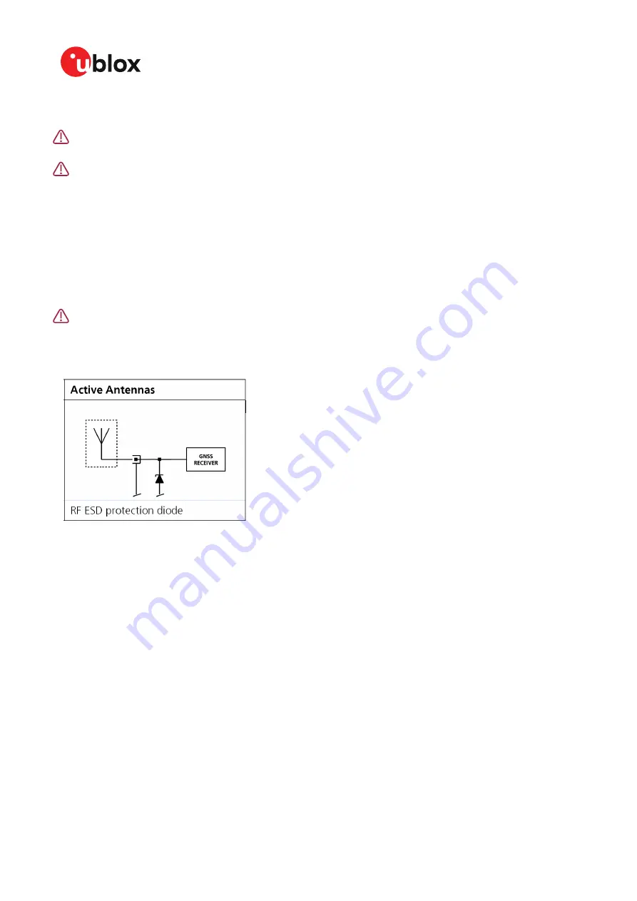
L-band receivers are sensitive to Electrostatic Discharge (ESD). Special precautions are
required when handling. Most defects caused by ESD can be prevented by following strict
ESD protection rules for production and handling. When implementing passive antenna
patches or external antenna connection points, then additional ESD measures as shown in
the figure below can also avoid failures in the field.
Figure 21: RF ESD precautions
4.5.2 EOS precautions
Electrical overstress (EOS) usually describes situations when the maximum input power exceeds
the maximum specified ratings. EOS failure can happen if RF emitters are close to a L-band receiver
or its antenna. EOS causes damage to the chip structures. If the RF_IN is damaged by EOS, it is hard
to determine whether the chip structures have been damaged by ESD or EOS.
EOS protection measures as shown in the figure below are recommended for any designs combining
wireless communication transceivers (e.g. GSM, GPRS) and L-band in the same design or in close
proximity.
UBX-19026111 - R07
4 Design
Page 31 of 52
C1-Public


