EVK-NORA-W1 - User guide
UBX-22002764 - R02
Hardware description
Page 18 of 22
C1-Public
shows the default configuration of
“
solder-bridge" jumpers. Choose alternative configurations
by cutting the bridge and soldering the jumpers in the default positions.
Jumper
Jumper type
Default function
Alternate function
J15
Solder-bridge
Connected to J20 debug connector, JTAG-TMS
Cut and close to Test Point GPIO42
J16
Solder-bridge
Connected to J20 debug connector, JTAG-TCK
Cut and close to Test Point GPIO39
J17
Solder-bridge
Connected to J20 debug connector, JTAG-TDO
Cut and close to Test Point GPIO40
J18
Solder-bridge
Connected to J20 debug connector, JTAG-TDI
Cut and close to Test Point GPIO41
J19
Solder-bridge
Connected to 32KHz clock, XT-32k-p
Cut and close to J2 connector GPIO15
J21
Solder-bridge
Connected to 32KHz clock, XT-32k-n
Cut and close to J2 connector GPIO16
Table 7: Solder-bridge jumpers overview
3.12
Header pin-out
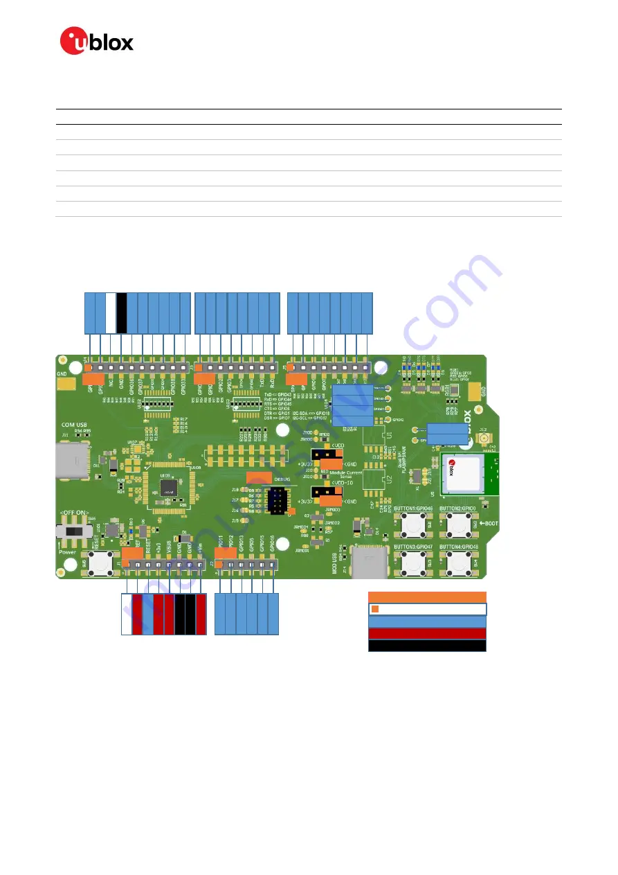
Figure 14
shows the 2.54 mm pitch sockets exposing the IO signals on the NORA-W10 module.
Figure 19: EVK-NORA-W10 headers
⚠
To enable the EVK-NORA-W10 I/O pins to handle 5 V signals the level shifters (U102
–
U104, TI
TXS0108EPWR) must be populated and
IOREF
must be supplied with +5 V. When using 3.3 V on
the EVK-NORA-W1 I/O pins, the Arduino Uno® style shields must be configured to use the +3.3 V
I/O voltage reference.
GPIO8
GPIO9
NC
.
IO
R
E
F
RE
S
E
T
+3
V
3
V
B
US
G
ND
G
ND
+V
in
G
P
IO
11
G
P
IO
12
G
P
IO
13
G
P
IO
5
G
P
IO
15
G
P
IO
16
G
P
IO
21
NC
G
ND
G
P
IO
36
G
P
IO
37
G
P
IO
35
G
P
IO
34
G
P
IO
38
G
P
IO
33
G
P
IO
10
G
P
IO
14
G
P
IO
2
G
P
IO
3
G
P
IO
4
G
P
IO
46
Tx
D
Rx
D
G
P
IO
45
G
P
IO
6
G
P
IO
1
G
P
IO
7
G
P
I04
7
G
P
IO
48
G
P
IO
18
G
P
IO
17
J1
J3
J4
J5
Headers
IO-signals
Color code
Supply voltage
Ground connection
GPIO42
GPIO41
GPIO40
GPIO39
J20
Pin-1 indicator
J2
J7
J8
G
P
IO
0


