UBX-14040040 - R20
C1-Public
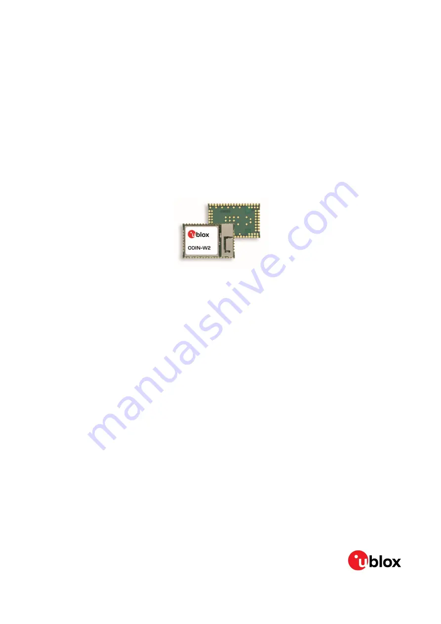
ODIN-W2 series
Stand-alone multiradio modules with
Wi-Fi and Bluetooth
System integration manual
Abstract
This document describes the system integration of ODIN-W2 series multiradio modules. The
ODIN-W2 module is a compact, stand-alone, dual-band Wi-Fi, Bluetooth
®
dual-mode (Bluetooth
BR/EDR v2.1 and Bluetooth Low Energy v4.0), multiradio module designed for Internet-of-Things
gateway applications.