SARA-G450 - System integration manual
UBX-18046432 - R08
System description
Page 15 of 143
C1-Public
1.5
Supply interfaces
1.5.1
Module supply input (VCC)
The modules must be supplied via the three VCC pins that represent the module power supply input.
The VCC pins are internally connected to the RF power amplifier and to the integrated Power
Management Unit: all supply voltages needed by the module are generated from the VCC supply by
integrated voltage regulators, including the V_BCKP Real Time Clock supply, V_INT digital interfaces
supply, and VSIM SIM card supply.
During operation, the current drawn by the SARA-G450 modules through the VCC pins can vary by
several orders of magnitude. This ranges from the high peak of current consumption during GSM
transmitting bursts at maximum power level in connected mode (as described in section
) to the
low current consumption during low power idle mode with power saving enabled (as described in
section
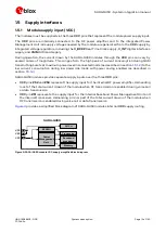
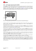
SARA-G450 modules provide separate supply inputs over the three VCC pins:
VCC pins #52 and #53 represent the supply input for the internal RF power amplifier, demanding
most of the total current drawn of the module when RF transmission is enabled during voice call
or data transmission
VCC pin #51 represents the supply input for the internal baseband Power Management Unit and
the internal transceiver, demanding a minor part of the total current drawn of the module when
RF transmission is enabled during voice call or data transmission
provides a simplified block diagram of SARA-G450 modules internal VCC supply routing.
53
VCC
52
VCC
51
VCC
SARA-G450
Power
Management
Unit
Memory
Baseband
processor
Transceiver
RF PMU
2G PA
Figure 3: SARA-G450 module VCC supply simplified block diagram


