Service Manual
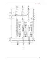
Function Block Diagram
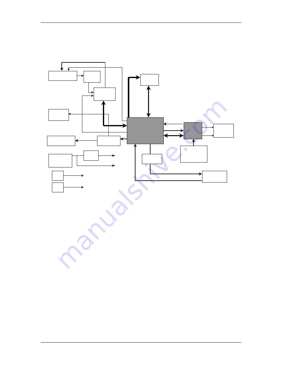
The following diagram reveals the functions of the scanner's main board.
CCD connector
LED
connector
MOTOR connector
POWER
JACK
ULN2003
Resistance
Gain
LM9811
DRAM
UTA connector
VIDE
O
DD0_7
LED_
N
RA0_8
RD0_7
NS_RS,NS_PH1,NS_PH2
(128,256K)
A,B,/A,/B
U_HOME,DETECT
U_A,B,/A,/B
MCLK
J1
J2
J3
J4
J7
M/B System Block Diagram
7805
+5V
+12V
R1,R2
TGI,SEL1,SEL2
U2
U4
Q4
U5
ASTRA 1220P
ASIC
S_CTR1_3
S_STATUS0_4
DA0_7
U1
74HC04
U6
CCD Processer
Data Storage
Motor Driver
Regulator
Scanner Function
EMI Reduce
ASTRA 1220U page 3
XTAL
24MHz
OSC
48MHz
U3
U4
X1
X2
U S B
PV8630
USB
Connector
D+
D -
93C46
Vendor ID
Fig. 2-3: System Block Diagram
5
Summary of Contents for Astra 1220U
Page 1: ...Astra 1220U Color Scanner Service Manual UMAX Data Systems Inc 0898 e...
Page 4: ...Pin Assignment 44 iv...
Page 14: ...Service Manual AD Pin Assignment 10...
Page 15: ...Service Manual Motor and To CCD Board Pin Assignment 11...
Page 16: ...Service Manual Power Code Pin Assignment 12...
Page 17: ...Service Manual EPP to USB Bridge Pin Assignment 13...
Page 19: ...Service Manual 3797P 15...
Page 37: ...Service Manual Appendix B Scanner Outline Diagram 312 83 98 471 33...


