background image


Electronic System


- 39 - 

Pin 1:   


DC +118V(+131V) 

  Pin 

2: 

  DC 

+49V(+11.5V) 

  Pin 

3: 

  DC 

+49V(+11.5V) 

Note:  When staring the Deuterium lamp, the voltage refer in the ( ). 

J8---To 

Tungsten 

Lamp 


Pin 1:   


DC +11V 

Pin 2:   


GND 

J9---From Main CPU PCB 


Pin 1, 2:  


DC +5V 

Pin 3:   


DC +3.85V(+5V) 

Pin 4:   


DC +5V(+3.85V) 

Note:  1. If the voltage of pin 3 is +3.85V, the Deuterium lamps is on, or 

it is off.   

2. If the voltage of pin 4 is +5V, the Tungsten lamps is on, or it is 

off. 

J10---To 2SC2625 of Tungsten Lamp   

Pin 1:   

DC +18V 

   Pin 

2:   DC 

+10.8V 

    Pin 

3: 

 DC 

+10.5V 

J11---To Cooling Fan  


Pin 1:   

DC +12V 

   Pin 

2:   GND 


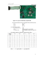
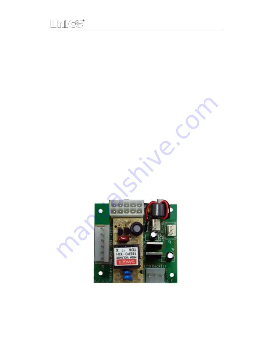
5.1.2  Power Distributing PCB(SST8.411.130A) 

The layout of the Power Distributing PCB is shown in figure 5.9 


Figure 5.9  Layout of Power Distributing PCB 

The sockets description of the Power Distributing PCB as follow: 

J1---From Switch Power Supply   


Pin 1:   


DC -12V 


Pin 2, 6, 7:   

DC +5V 

Summary of Contents for SQ Series

Page 1: ...UV 2800 UV 2802 UV 2802PC UV 2802S UV 2802PCS UV 3802 UV 4802 SPECTROPHOTOMETER SERVICE MANUAL UNICO 182 Ridge Road Suite E Dayton NJ 08810 USA 732 274 1155 Fax 732 274 1151 WEB www unicosci com E ma...

Page 2: ...System 25 4 1 Incidence of Light 25 4 2 Dispersion of Light 25 4 3 Exit of Light 25 4 3 1 Exit of the Single Beam UV 2800 UV 2802 UV 2802S 25 4 3 2 Exit of the Split Beam UV 3802 25 4 3 3 Exit of the...

Page 3: ...emory check failed 58 6 4 Printer check failed 58 6 5 Filter positioning failed 59 6 6 Light source positioning failed 60 6 7 Auto cell positioning failed 61 6 8 Slit positioning failed 62 6 9 Search...

Page 4: ...eplace Memory Battery 77 7 5 Upgrade Firmware 78 7 6 Check Performance 81 7 6 1 Prepare 81 7 6 2 Check Wavelength Accuracy 81 7 6 3 Check Stray Light 82 7 6 4 Check Absorbance Accuracy 82 7 6 5 Check...

Page 5: ......

Page 6: ...e analytical grating system has 1200 grooves mm for high spectral dispersion The models UV 2800 UV 2802 UV 2802PC UV 2802S and UV 2802PCS are Single Beam the model UV 3802 is Split Beam and the model...

Page 7: ...Introduction 2 Figure 1 2 Model UV 2802 UV 2802S Figure 1 3 Model UV 2802PC UV 2802PCS Figure 1 4 Model UV 3802...

Page 8: ...Introduction 3 Figure 1 5 Model UV 4802...

Page 9: ...3nm 620X400X280 21kg UV 2800 Single beam grating system1200 lines mm 4nm 190 1100nm 0 8nm 0 5nm LCD 320 240 DMF50083 0 15 T 220nm 340nm 0 200 T 0 3 3 0A 0 9999C 0 5 T 0 002A h 500nm 0 004A Tungsten l...

Page 10: ...sh Rod 23 Shield Cover 24 Photo couple2 Filter 25 Motor3 Filter 26 Amplifier PCB 27 Condenser Lens 28 4 cell Sample Holder 29 Sample Compartment 30 Slave CPU PCB 31 Lamp Source Room 32 Auto cell Chang...

Page 11: ...Layout 6 1 2 3 4 5 6 7 8 9 10 11 12 13 14 15 16 17 18 19 20 21 25 24 23 22 29 28 27 26 33 32 31 30 34 Figure 3 1 Layout of UV 2800 Inside Top View...

Page 12: ...Layout 7 Figure 3 2 Layout of UV 2800 Inside Bottom View...

Page 13: ...Layout 8 39 40 41 42 43 Figure 3 3 Layout of UV 2800 Top View...

Page 14: ...Layout 9 230V 44 45 46 47 48 49 50 51 Figure 3 4 Layout of UV 2800 Back View...

Page 15: ...Photo coupler2 Filter 26 Motor3 Filter 27 Shield Cover 28 Amplifier PCB 29 Condenser Lens 30 Sample Compartment 31 Slit Switch Equipment 32 4 Cell Sample Holder 33 Photo coupler4 Slit 34 Motor4 Slit 3...

Page 16: ...Layout 11 35 32 30 29 28 27 26 25 24 23 1 2 3 4 5 6 7 8 9 10 11 12 13 14 15 16 17 18 19 20 21 22 38 37 36 Figure 3 5 Layout of UV 2802 UV 2802PC Inside Top View...

Page 17: ...Layout 12 35 34 33 32 31 30 29 28 27 26 25 24 23 1 2 3 4 5 6 7 8 9 10 11 12 13 14 15 16 17 18 19 20 21 22 38 37 36 Figure 3 6 Layout of UV 2802S UV 2802PCS Inside Top View...

Page 18: ...Layout 13 Figure 3 7 Layout of UV 2802 S UV 2802PC S Inside Bottom View...

Page 19: ...Layout 14 43 44 45 46 47 Figure 3 8 Layout of UV 2802 S Top View...

Page 20: ...Layout 15 230V Figure 3 9 Layout of UV 2802 S UV 2802PC S Back View...

Page 21: ...l Push Rod 25 Photo coupler2 Filter 26 Motor3 Filter 27 Shield Cover 28 Main Amplifier PCB 29 Condenser Lens 30 Sample Compartment 31 Light Distribute Room 32 4 Cell Sample Holder 33 Condenser Lens 34...

Page 22: ...Layout 17 35 32 30 29 28 27 26 25 24 23 1 2 3 4 5 6 7 8 9 10 11 12 13 14 15 16 17 18 19 20 21 22 38 36 31 33 34 37 39 Figure 3 10 Layout of UV 3802 Inside Top View...

Page 23: ...Layout 18 Figure 3 11 Layout of UV 3802 Inside Bottom View...

Page 24: ...Layout 19 44 45 46 47 48 Figure 3 12 Layout of UV 3802 Top View...

Page 25: ...Layout 20 230V Figure 3 13 Layout of UV 3802 Back View...

Page 26: ...r 24 Pull Push Rod 25 Photo coupler2 Filter 26 Motor3 Filter 27 Shield Cover 28 Main Amplifier PCB 29 Condenser Lens 30 Sample Compartment 31 Light Distribute Room 32 Sample Holder 33 Slave Amplifier...

Page 27: ...Layout 22 35 32 30 29 28 27 26 25 24 23 1 2 3 4 5 6 7 8 9 10 11 12 13 14 15 16 17 18 19 20 21 22 38 36 31 33 34 37...

Page 28: ...Layout 23 Figure 3 14 Layout of UV 4802 Inside Top View...

Page 29: ...Layout 24 Figure 3 15 Layout of UV 4802 Inside Bottom View...

Page 30: ...Layout 25 43 44 45 46 47 Figure 3 16 Layout of UV 4802 Top View...

Page 31: ...Layout 26 230V Figure 3 17 Layout of UV 4802 Back View...

Page 32: ...ondenser lens focused on the sample continue pass through the sample the light finally to the photodetector Shown in Figure 4 1 4 3 2 Exit of the Split Beam UV 3802 From the exit slit the light was se...

Page 33: ...ror Deuterium Mirror Slit Concave Mirror Collimatng Mirror Grating Filter Slit Condenser Lens Sample Photodetector Condenser Lens Figure 4 1 Optical System schematic diagram of UV 2800 UV 2802 UV 2802...

Page 34: ...Deuterium Mirror Slit Concave Mirror Collimatng Mirror Grating Filter Slit Condenser Lens Sample Photodetector Condenser Lens Prismatic Mirror Condenser Lens Photodetector Figure 4 2 Optical System sc...

Page 35: ...Optical 30 Figure 4 3 Optical System schematic diagram of UV 4802...

Page 36: ...J11 J9 PCB SST8 411 128A J2 J3 J4 J5 J1 J6 J7 J8 J10 J11 J9 Pur Red Blu Blk Yel Org Gry Wht Cooling Fan Rectifier Transistor1 Tungsten Lamp Deuterium Lamp Transistor2 GND Yel Grn Yel Grn Yel Grn Wht B...

Page 37: ...J1 J6 J7 J8 J10 J11 J9 Pur Red Blu Blk Yel Org Gry Wht Cooling Fan Rectifier Transistor1 Tungsten Lamp Deuterium Lamp Transistor2 GND Yel Grn Yel Grn Yel Grn Wht Brw Org R ed J1 J2 PCB SST8 413 104A J...

Page 38: ...u Blk Yel Org Gry Wht Cooling Fan Rectifier Transistor1 Tungsten Lamp Deuterium Lamp Transistor2 GND Yel Grn Yel Grn Yel Grn Wht Brw Org R ed J1 J2 PCB SST5 413 104A J1 J2 J1 J3 PCB SST8 412 314A J1 J...

Page 39: ...J6 J7 J8 J10 J11 J9 Pur Red Blu Blk Yel Org Gry Wht Cooling Fan Rectifier Transistor1 Tungsten Lamp Deuterium Lamp Transistor2 GND Yel Grn Yel Grn Yel Grn Wht Brw Org R ed J1 J2 PCB SST8 413 104A J1...

Page 40: ...J7 J8 J10 J11 J9 Pur Red Blu Blk Yel Org Gry Wht Cooling Fan Rectifier Transistor1 Tungsten Lamp Deuterium Lamp Transistor2 GND Yel Grn Yel Grn Yel Grn Wht Brw Org R ed J1 J2 PCB SST8 413 104A J1 J2...

Page 41: ...Electronic System 36 5 1 Power Supply System Figure 5 6 Power Supply schematic diagram of UV 2800 UV 2802 UV 2802PC UV 2802S UV 2802PCS...

Page 42: ...ic diagram of UV 3802 UV 4802 The power supply system of the SQ series are made up of two parts the transformer supplied for the light source as Tungsten lamp and Deuterium lamp and the Switch Power S...

Page 43: ...of Power Supply PCB The sockets description of the Power Supply PCB as follow J1 To Rectifier Pin 1 DC 18V Pin 2 3 AC 15V J2 From Transformer Pin 1 2 AC 15V J3 From Transformer Pin 1 4 AC 18V Pin 2 5...

Page 44: ...e Deuterium lamps is on or it is off 2 If the voltage of pin 4 is 5V the Tungsten lamps is on or it is off J10 To 2SC2625 of Tungsten Lamp Pin 1 DC 18V Pin 2 DC 10 8V Pin 3 DC 10 5V J11 To Cooling Fan...

Page 45: ...CPU on Main CPU PCB command the motor to goto the setup wavelength select the correct light source and filter 2 Halogen or deuterium lamp to supply the light the Monochromator to isolate the wavelengt...

Page 46: ...ompar tment Sampling and Pre amplifier A D and Signal Process Main Control System Keypad LCD Display Printer Port RS 232 Turn on off Light Souce Switch Light Source Go WL Select Filter Go Auto Sample...

Page 47: ...mpling and Pre amplifier Slave A D and Signal Process Main Control System Keypad LCD Display Printer Port RS 232 Turn on off Light Souce Switch Light Source Go WL Select Filter Go Auto Sample Holder S...

Page 48: ...Process Main Control System Keypad LCD Display Printer Port RS 232 Turn on off Light Souce Switch Light Source Go WL Select Filter Go Auto Sample Holder Sampling and Pre amplifier Slave Figure 5 12 W...

Page 49: ...Electronic System 44 Figure 5 13 Layout of Main CPU PCB...

Page 50: ...put signal from Keypad CZ5 To Printer Port Pin 1 Pulse for read the data for printer Pin 2 9 Data bus Pin 10 Error detect 5V indicate the printer is OK Pin 11 Busy detect 5V indicate the printer is bu...

Page 51: ...r Pin 5 Slit Photo coupler signal Pin 6 Wavelength Photo coupler and limit switch signal Pin 7 Filter Photo coupler signal Pin 8 Lamp limit switch signal Pin 9 11 13 15 GND Pin 10 12 14 16 DC 12V CN2...

Page 52: ...2802 UV 2802PC UV 3802 UV 4802 Drive PCB The sockets description of the Drive PCB as follow CN1 From Main CPU PCB Pin 1 4 Control slit step motor Pin 5 Slit Photo coupler signal Pin 6 Wavelength Photo...

Page 53: ...or Pin 5 DC 12V J7 To slit step motor Pin 1 4 Drive slit step motor Pin 5 DC 12V J9 To filter Photo coupler Pin 1 GND Pin 2 DC 5V 0V 0V only at initiative position Pin 3 DC 1 2V J11 To slit Photo coup...

Page 54: ...PU PCB Pin 1 8 Output signal to Keypad Pin 9 12 Input signal from Keypad CZ41 To keypad Pin 1 8 Output signal to Keypad Pin 9 12 Input signal from Keypad CZ6 From Main CPU PCB Pin 1 4 13 Control signa...

Page 55: ...Slave CPU send the digital signal to the main CPU 5 3 1 Amplifier PCB SST8 413 104A The layout of the Amplifier PCB of UV 2800 UV 2802 UV 2802PC UV 2802S and UV 2802PCS R17 R20 of UV 2802S and UV 2802...

Page 56: ...7 0 0 0 0 0 0 1 0 1 0 0 0 2 1 0 0 0 0 3 1 1 0 0 0 4 1 1 0 0 1 5 1 1 0 1 0 6 1 1 0 1 1 7 1 1 1 0 0 8 1 1 1 0 1 9 1 1 1 1 0 10 1 1 1 1 1 Note 1 0 Logic low 0V 1 Logic high 5V The amplifier multiple of U...

Page 57: ...1 2 3 5 7 9 11 13 15 GND Pin 4 Analog signal from pin 6 of OP07 Pin 16 DC 5V Pin 6 8 10 12 14 Control amplifier multiple from Slave CPU PCB The amplifier multiple of UV 4802 Amplifier PCB as follow A...

Page 58: ...the slave Amplifier PCB of UV 3802 as follow J1 From Power Distributing PCB Pin 1 DC 9V Pin 2 GND Pin 3 DC 9V J2 From Slave CPU PCB Pin 1 GND Pin 2 DC 5V Pin 3 4 Control amplifier multiple from Slave...

Page 59: ...3 5 7 9 11 13 GND Pin 4 Analog signal from pin 6 of OP07 Pin 6 8 10 12 14 Control amplifier multiple from Slave CPU PCB The amplifier multiple of UV 4802 slave Amplifier PCB as follow Amplifier multip...

Page 60: ...c System 55 5 3 3 Slave CPU PCB SST8 412 314 The layout of the slave CPU PCB is shown in figure 5 22 5 23 5 24 Figure 5 22 Layout of UV 2800 UV 2802 S Slave CPU PCB Figure 5 23 Layout of UV 3802 Slave...

Page 61: ...B Pin 1 GND Pin 2 Analog signal from pin 6 of OP07 Pin 3 4 Control amplifier multiple of Slave Amplifier PCB J3 To Amplifier PCB Pin 1 GND Pin 2 Analog signal from pin 6 of OP07 Pin 8 DC 5V Pin 3 7 Co...

Page 62: ...5 7 9 11 13 GND Pin 4 Analog signal from pin 6 of OP07 Pin 6 8 10 12 14 Control amplifier multiple of Slave Amplifier PCB J3 To Amplifier PCB Pin 1 2 3 5 7 9 11 13 15 GND Pin 4 Analog signal from pin...

Page 63: ...Trouble Shooting 58 6 Trouble Shooting 6 1 Tungsten lamp off...

Page 64: ...T8 411 128A OK 1 Solving the wiring of J5 on PCB SST8 411 128A 2 Replace transformer DC 3 85V on pin 2 of CZ7 on PCB SST8 412 113 OK Solving the wiring from CZ7 to J9 on PCB SST8 411 128A Replace PCB...

Page 65: ...Trouble Shooting 60 6 3 Memory check failed 6 4 Printer check failed Note It is recommended to connect the M501 to printer with cable after both are powered on...

Page 66: ...04 3 Replace PCB SST8 414 103 104 4 Replace filter motor 5 Replace PCB SST8 412 113 DC 1 2V on pin 3 of J9 on PCB SST8 414 103 104 OK 1 Solving the wiring CN1 on PCB SST8 414 103 104 to PCB SST8 412 1...

Page 67: ...g of CN2 on PCB SST8 414 103 104 3 Replace PCB SST8 414 103 104 4 Replace light change motor 5 Replace PCB SST8 412 113 1 Solving the wiring CN1 on PCB SST8 414 103 104 to PCB SST8 412 113 2 Replace P...

Page 68: ...positioning Y N 1 Solving the wiring from auto cell holder to auto cell holder connector 2 Solving the wiring from auto cell holder connector to J3 on PCB SST8 412 113 3 Replace auto cell holder moto...

Page 69: ...Trouble Shooting 64 6 8 Slit check failed Only for UV 2802S UV 2802PCS...

Page 70: ...mple compartment N Take it away Y Deuterium lamp on N Refer 6 2 Light Source positioning OK Y Filter positioning OK Y Refer 6 6 Refer 6 5 N Wavelength motor works OK Y 1 Solving the wiring of waveleng...

Page 71: ...h Y N 1 Solving the wiring of J14 on PCB SST8 414 103 104 2 Solving the wiring of CN2 on PCB SST8 414 103 104 3 Replace photo coupler 4 Replace PCB SST8 411 103 104 5 Replace IC 8255 of U17 on PCB SST...

Page 72: ...Trouble Shooting 67 6 13 Get dark current for a long time...

Page 73: ...power socket to the switch power Power on N Connect power cord N Replace fuse N Y AC 1200V of J3 on PCB SST8 417 100 OK AC 1200V of J3 on PCB SST8 411 130A OK 5V of J1 on PCB SST8 411 130A OK Y 5V of...

Page 74: ...Trouble Shooting 69 6 15 Backlight OK but display nothing on LCD Display...

Page 75: ...Trouble Shooting 70 6 16 Energy low warning after blanking Note If measuring at less than 200nm or more than 1000nm it is possible to appear Energy low warning...

Page 76: ...uvette N Anything block off the beam in the sample compartment N Take it away Y Dilute reference or sample solution Y Y Replace tungsten lamp Vis area or deuterium lamp UV area Filter positioning OK R...

Page 77: ...Trouble Shooting 72 6 18 No DC 12V on PCB SST8 412 113...

Page 78: ...stability is greater than 10 and the frequency stability is greater than 1 of the power supply no strong magnetic field near the instrument Always allow the instrument to warm up for 20 minutes prior...

Page 79: ...Maintenance 74 Figure 7 1 Remove the cover screws 4 Very carefully remove the cover of the instrument and place in right side of the instrument Show in Figure 7 2 Figure 7 2 Remove the cover...

Page 80: ...ctors CZ6 CZ4 and J3 on PCB marked SST8 417 100 Be sure to reconnect after replacing the lamp Show in Figure 7 3 Figure 7 3 Unplug J3 CZ4 CZ6 5 Remove the grey metal protection cover Using screwdriver...

Page 81: ...base 7 Insert the new lamp Figure 7 5 pushing it in as far as it will go Figure 7 5 Tungsten Lamp 8 Re fit the grey metal protection cover temporarily re fit the main cover and fix with two screws one...

Page 82: ...grey protection cover and turn on the instrument Adjust to make the image central on the slit Install the grey metal protection cover and instrument cover Figure 7 6 Adjust Tungsten Lamp CAUTION DO N...

Page 83: ...amp bracket to the instrument base Pull the entire lamp and lamp holder assembly out Shown in Figure 7 7 Figure 7 7 Take off the Deuterium Lamp 3 Replace the pre aligned lamp with a lamp Figure 7 8 pr...

Page 84: ...t the lamp alignment needs adjustment This requires running the SQ series without the covers with high voltages accessible and so should only be performed by a suitably qualified engineer If adjustmen...

Page 85: ...place Memory Battery 1 Turn the spectrophotometer upside down onto a padded surface Remove the all screws around the sides of the spectrophotometer shown in Figure 7 10 and take away the bottom cover...

Page 86: ...er and keep it on for a few minutes 5 Turn off the spectrophotometer 6 Immediately after turning off the spectrophotometer remove the old battery and insert the new one This MUST be completed within 3...

Page 87: ...py the folder Update UNICO provided to the disk C of your computer Usually there are five files in the folder Update which are respectively Flash UNICO exe H00 H01 H02 and H03 H00 H01 H02 and H03 is d...

Page 88: ...n only select the file H00 in the folder Update click on Open to load 8 Turn on spectrophotometer the screen will display as below Figure 7 14 and wait for upgrading Figure 7 14 Upgrade State 9 Click...

Page 89: ...he normal position 12 Turn on the spectrophotometer it will run with the new software 13 It is highly recommended that following software upgrading you select calibration system after the self testing...

Page 90: ...n complete press F3 Search Press record wavelength of didymium peak specification 807 1 1nm 7 6 3 Check Stray Light 1 Prepare Refer 7 6 1 2 Press Set input 340 press Enter to go to 340nm 3 Ensure beam...

Page 91: ...ould be greater than or equal to 1 The maximum at Gain 10 should be 2000 to 4000 7 6 6 Check Energy Profile 1 Prepare Refer 7 6 1 2 Press 3 to select WL Scan press F1 to setup set the parameter as fol...

Page 92: ...414 012 SST8 414 103 SQ5 417 006 SST8 417 100 SQ5 415 007 SST8 417 101 SQ5 415 008 SST8 417 102 SQ6 491 317 Cooling Fan SQ6 491 314 Transistor1 W Lamp SQ6 491 313 Transistor2 D2 Lamp SQ0 001 001 Recti...

Page 93: ...SST8 417 100 SQ5 415 007 SST8 417 101 SST8 415 001 B SQ5 415 005 SST8 415 001 D SQ6 491 341 Cooling Fan SQ6 491 314 Transistor1 W Lamp SQ6 491 313 Transistor2 D2 Lamp SQ0 001 001 Rectifier SQ6 491 335...

Page 94: ...0 SQ5 415 007 SST8 417 101 SST8 415 001 B SQ5 415 005 SST8 415 001 D SQ6 491 341 Cooling Fan SQ6 491 314 Transistor1 W Lamp SQ6 491 313 Transistor2 D2 Lamp SQ0 001 001 Rectifier SQ6 491 335 Motor1 Lam...

Page 95: ...04 SQ5 417 006 SST8 417 100 SQ5 415 007 SST8 417 101 SST8 415 001 B SQ5 415 005 SST8 415 001 D SQ6 491 341 Cooling Fan SQ6 491 314 Transistor1 W Lamp SQ6 491 313 Transistor2 D2 Lamp SQ0 001 001 Rectif...

Page 96: ...4 104 SQ5 417 006 SST8 417 100 SQ5 415 007 SST8 417 101 SST8 415 001 B SQ5 415 005 SST8 415 001 D SQ6 491 341 Cooling Fan SQ6 491 314 Transistor1 W Lamp SQ6 491 313 Transistor2 D2 Lamp SQ0 001 001 Rec...

Reviews: