User’s Manual
19
Header for Case Panel
J2
IDE 1 LED
J2
Pin 1, Pin 2
IDE 2 LED
J2
Pin 3, Pin 4
External Speaker
J2
Pin 5, Pin 8
Buzzer On/Off
J2
Pin 6, Pin 7
Hardware Reset Switch
J2
Pin 9, Pin 10
Power LED
J2
Pin 13, Pin 14
ATX Power Supply On/Off Switch
J2
Pin 15, Pin 16
Turbo LED (for case only, no function)
J2
Pin 17, Pin 18
ATX or PS/2 Power Selector
J2
Pin 19, Pin 20, Pin 21
Ring-Detected
J2
Pin 22, Pin 23
CPU Type Setting: JP19 / JP18
JUMPER No
.
CPU Type
JP19
(1-2)
JP19
(3-4)
JP19
(5-6)
JP18
(7-8)
JP18
(5-6)
Intel 0.25u
Celeron
SHORT OPEN OPEN SHORT
OPEN
Intel 0.18u
Celeron
Coppermine
OPEN SHORT OPEN SHORT
OPEN
VIA / Cyrix
SHORT OPEN SHORT
OPEN SHORT
Note: CPU ratio already locked by CPU internally.
System Clock Setting: JP17
JP17 (1-2)
JP17 (3-4)
CPU BUS
CLOCK
PCI BUS CLOCK
OPEN
OPEN
133 MHz
33.3 MHz
OPEN
CLOSE
100 MHz
33.3 MHz
CLOSE CLOSE 66
MHz 33
MHz
Caution:
Please make sure the CPU type setting and System clock setting as
mention above for your system. Any wrong setting may cause
system damaged the CPU or system not working.
20
The ENDAT-3701/3702/3902 All-In-One motherboard
JP10: CMOS Data Clear:
Pin 1-2 *
Normal
Pin 2-3
Clear CMOS Data
JP11: DiskOnChip Memory Address Selector
JP11
Memory Address
1-2 7-8
0 C 8 0 0 H - 0C9FFH
1-2 9-10
0CC00H - 0CDFFH
3-4 7-8
0D000 H - 0D1FFH
3-4 9-10
0D400 H - 0D5FFH
*5-6 *7-8
0D800H - 0D9FFH
JP8: On-board LAN Disable/Enable
Pin 1-2 *
Enable On-Board LAN
Pin 2-3
Disable On-Board LAN
JP12 / JP22: Flash ROM Size/Voltage selector.
JP12 FLASH ROM SIZE
1-2=2MB *2-3=4MB
JP22 FLASH ROM Voltage
1-2= 5V Type
*2-3=3.3V Type
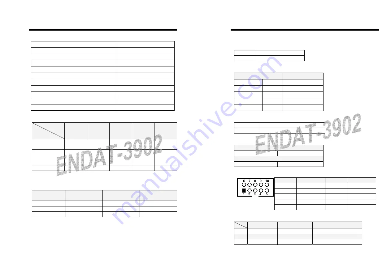
Box Header: COM1(CN9)/COM2(CN7)/COM3(CN11)/COM4(CN12)
Pin No.
Description
Pin No.
Description
1 DCD 6 DSR
2 RXD 7 RTS
3 TXD 8 CTS
4 DTR 9
RI
/
PWR
5 GND 10 N.C.
JP1: Voltage selector for COM1, COM2
COM1
COM2
Description
JP1
Close 1-2
Close 7-8
+5V
JP1
Close 3-4
Close 9-10
STD. RI. (RS-232)
JP1
Close 5-6
Close 11-12
+12V


