background image

ENDAT

N3410


User’s


Manual


UNICORN


COMPUTER


CORP.


Copyright 2015 Unicorn Computer Corporation. All rights reserved. 

28 


state.  

3.


Onboard


3.1.


Connectors and Headers   

CAUTION


Only the following connectors and headers have over current protection: back panel and front panel 

USB.  


• Back panel connectors   

This section describes the board’s connectors and headers. The connectors and headers can be divided 

into these groups: 

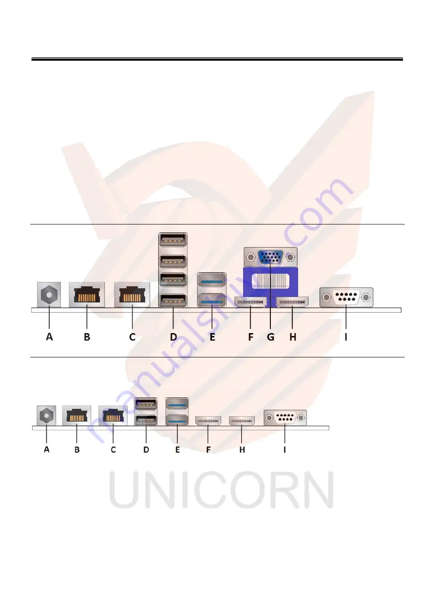
Figure


7


&


figure


8


shows


the


location


of


the


back


panel


connector


for


the


board


Figure 7 – Rear I/O 


Figure 8 – Rear I/O for N3410S 


Summary of Contents for ENDAT-N3410

Page 1: ...ENDAT N3410 User s Manual UNICORN COMPUTER CORP Copyright 2015 Unicorn Computer Corporation All rights reserved 1 ENDAT N3410 For ENDAT N3410 PCB ver A01 Document version 0 7 Release Date Mar 08 2016 ...

Page 2: ... registered trademark of Intel Corporation VIA is registered trademark of VIA Technology Incorporation Plug and Play is registered trademarks of Intel Corporation Microsoft Windows and MS DOS are trademarks of Microsoft Corporation Award is a trademark of Phoenix Software Inc PCI is a registered trademark of PCI Special Interest Group Other product names mentioned herein are used for identificatio...

Page 3: ... 9 1 3 COMPONENTS LIST 11 1 4 BLOCK DIAGRAM 12 2 TECHNICAL REFERENCE 13 2 1 PROCESSOR 13 2 2 SYSTEM MEMORY 14 2 3 MEMORY RESOURCES 16 2 4 PROCESSOR GRAPHICS SUBSYSTEM 17 2 4 1 INTEGRATED GRAPHICS 17 2 5 USB 3 0 AND 2 0 HOST CONTROLLER 18 2 5 1 USB 3 0 PORTS 18 2 5 2 USB 2 0 PORTS 18 2 6 SATA INTERFACE 19 2 7 REAL TIME CLOCK SUBSYSTEM 20 2 8 AUDIO SUBSYSTEM 21 2 9 LAN SUBSYSTEM 22 2 10 HARDWARE MON...

Page 4: ...nual UNICORN COMPUTER CORP Copyright 2015 Unicorn Computer Corporation All rights reserved 4 3 1 CONNECTORS AND HEADERS 28 3 2 JUMPER SETTING 31 3 3 PIN HEADER DEFINED 34 4 APPENDIX 45 4 1 WDT AND DIGITAL I O PROGRAMMING 45 ...

Page 5: ... ITX boards with Intel Braswell SOC Sep 30 2015 0 2 Fix description errors Oct 02 2015 0 3 Changed power input voltages to 9 35V Oct 05 2015 0 4 Add programming guide for GPIO and WDT function Dec 17 2015 0 5 Modified information and add connector defined for VGA and JFP1 Feb 25 2016 0 6 Add procedure for BIOS refresh Mar 06 2016 0 7 Changed label for KB MS and Audio Line in Mar 08 2016 ...

Page 6: ...corn Computer Unicorn Computer Corporation may have patents or pending patent applications trademarks copyrights or other intellectual property rights that relate to the presented subject matter The furnishing of documents and other materials and information does not provide any license express or implied by estoppel or otherwise to any such patents trademarks copyrights or other intellectual prop...

Page 7: ...ly the ENDAT N3410S contains is for slim type design support The Unicorn Computer ENDAT N3410 series is allowing operation from 20 to 60 C without active cooling The wide power input range of 9 to 35VDC also provides flexibility across various DC power sources Device drivers are available at http www unicorn computer com tw For additional information call Technical Support at 886 2 2223 6699 You c...

Page 8: ...witch by jumper select GPIO 8 bit in out Serial 4 Serial Ports w 5 12V Power select COM2 COM3 support RS232 422 485 by System BIOS the COM2 COM4 are box header type USB 2 0 USB 3 0 8 USB ports include 6 USB 2 0 2 USB 3 0 Other 2 x POE EXPANSION SLOT 2 mini PCIe socket design with One Full and One Half 2 x PoE RJ 45 connector COM1 2 x HDMI 1 x VGA For ENDAT N3410 USB 2 0 x 4 ENDAT N3410S USB2 0 x 2...

Page 9: ...N COMPUTER CORP Copyright 2015 Unicorn Computer Corporation All rights reserved 9 1 2 Board Layout Show the location of the major components on the top side of Unicorn Board ENDAT N3410 Figure2 Board Components Represents the 1st Pin ...

Page 10: ...be divided Figure 3 Rear I O for N3410 Figure 4 Rear I O for N3410S Item Description A DC 9 V to 35 V Power Jack B Ethernet RJ 45 Without LED C Ethernet RJ 45 Without LED D Four or Two Port USB 2 0 Connector Option by model number T Two Port USB 3 0 Connector F HDMI1 Connector DDI0 G VGA Connector DDI2 this for N3410 only H HDMI2 Connector DDI1 Option Switch LVDS by H W BOM Changed I Serial Port1 ...

Page 11: ... 2 JP7 for and power select via pin 9 of JCOM1 2 JP8 LVDS back light select JFP1 Front Panel Power LED External Buzzer Reset PWBTN SIO Enabled select JMPCIEVER1 Mini PCI Slot 1 1 and 2 0 select J1 MIC Line In audio connector J2 Speaker LM1877Amplifier audio connector J3 Digital I O header JKBMS Keyboard Mouse header JCPUFAN1 Processor fan header JSYSFAN1 System fan header SMB1 SM bus Header JCOM2 ...

Page 12: ... N3410 User s Manual UNICORN COMPUTER CORP Copyright 2015 Unicorn Computer Corporation All rights reserved 12 1 4 Block Diagram Block diagram of the major functional areas of the board Figure5 Block Diagram ...

Page 13: ...rated graphics Integrated memory controller Integrated PCH Processor Number N3700 N3000 N3050 N3150 Cache 2 MB L2 Cache 2 MB L2 Cache 2 MB L2 Cache 2 MB L2 Cache Instruction Set 64 bit 64 bit 64 bit 64 bit Lithography 14 nm 14 nm 14 nm 14 nm of Cores 4 2 2 4 of Threads 4 2 2 4 Processor Base Frequency 1 6 GHz 1 04 GHz 1 6 GHz 1 6 GHz Burst Frequency 2 4 GHz 2 08 GHz 2 16 GHz 2 08 GHz TDP 6 W 4 W 6...

Page 14: ... system memory 1024 MB Non ECC SO DIMMs Serial Presence Detect NOTE If you install 1333 MHz it will run at 1066 MHz Supported Memory Configurations SO DIMM Capacity Configuration Note SDRAM Density SDRAM Organization Front side Back side Number of SDRAM Devices 1024 MB SS 1 Gbit 128 M x8 empty 8 2048 MB DS 1 Gbit 128 M x8 128 M x8 16 2048 MB SS 2 Gbit 256 M x8 empty 8 4096 MB DS 2 Gbit 256 M x8 25...

Page 15: ...rst 2 If the DIMM does not go in smoothly do not force it Pull it all the way out and try again B Memory Capacity DIMM Socket Location DDR3L Module Total Memory Size DIMMA1 512MB 1GB 2GB 4GB 8GB DIMMB1 512MB 1GB 2GB 4GB 8GB Max is 8GB C Dual Channel Memory Installation Please refer to the following requirements to activate Dual Channel function Install memory module of the same density in pairs sh...

Page 16: ...ress space being allocated for other system critical functions These functions include the following BIOS SPI Flash device 64 Mbit Local APIC 19 MB Direct Media Interface 40 MB PCI Express configuration space 256 MB SoC base address registers PCI Express ports up to 256 MB Memory mapped I O I O fabric that is dynamically allocated for PCI Express add in cards 256 MB The board provides the capabili...

Page 17: ... Video Memory Technology DVMT is a method for dynamically allocating system memory for use as graphics memory to balance 2D 3D graphics and system performance If your computer is configured to use DVMT graphics memory is allocated based on system requirements and application demands up to the configured maximum amount When memory is no longer needed by an application the dynamically allocated port...

Page 18: ... are implemented with external back panel connectors Black Maximum current is 500 mA for each port 2 A total Two ports via one dual port internal 1x8 1 25 mm pitch header Black Maximum current is 500 mA for each port of the header 1 A total Two ports via two dual port internal Mini Card Slot Maximum current is 500 mA for each port of the Mini Card Socket 1 A total All the USB ports are high speed ...

Page 19: ...de for configurations using Windows operating systems AHCI Mode The board supports AHCI storage mode NOTE In order to use AHCI modes AHCI mode force enabled in the BIOS Microsoft Windows 8 includes the necessary AHCI drivers without the need to install separate AHCI drivers during the operating system installation process However it is always good practice to update the AHCI drivers to the latest ...

Page 20: ... the computer is plugged in the standby current from the power supply extends the life of the battery The clock is accurate to 13 minutes year at 25 ºC with 3 3 VSB applied via the power supply 5 V STBY rail NOTE 1 If the battery and AC power fail date and time values will be reset and the user will be notified during the POST 2 When the voltage drops below a certain level the BIOS Setup program s...

Page 21: ...phone Analog Microphone jack on the front panel High Definition Audio via a stereo microphone headphone jack on the back panel Support for 44 1 kHz 48 kHz 96 kHz 192 kHz sample rates on all analog outputs Support for 44 1 kHz 48 kHz 96 kHz sample rates on all analog inputs Internal 2 00mm header support Line in Line out MIC in Speaker Pins Define Speakers Headphones Microphone Line In Audio Softwa...

Page 22: ...s RJ 45 LAN connector without integrated status LEDs 10 100 1000 BASE T IEEE 802 3 compliant Additional features of the LAN subsystem include CSMA CD protocol engine Jumbo frame support 9K LAN connect interface between the SoC and the LAN controller Power management capabilities ACPI technology support LAN wake capabilities Support POE PD function support TCP IP and UDP checksum offload for IPv4 a...

Page 23: ... rights reserved 23 2 10 Hardware Monitoring The hardware monitoring and fan control subsystem is based on Nuvoton embedded controller which supports the following Processor and system ambient temperature monitoring Chassis fan speed monitoring Voltage monitoring of 12v 5 V 3 3 V SM Bus interface ...

Page 24: ... to power off the computer Support for multiple wake up events Support for a front panel power and sleep mode switch by OS setting Lists the system states based on how long the power switch is pressed depending on how ACPI is configured with an ACPI aware operating system If the system is in this state And the power switch is pressed for The system enter this state Off ACPI G2 G5 Soft off Less tha...

Page 25: ...sed can be turned off The operating system uses information from applications and user settings to put the system as a whole into a low power state List the power states supported by the board along with the associated system power targets See the ACPI specification for a complete description of the various system and power states Table 5 Power States and Targeted System Power Notes 1 Total system...

Page 26: ... to remain in sleep state USB S3 S4 Note 3 4 Wake S4 controlled by BIOS option PCIe via WAKE S3 S4 Note 1 Via WAKE monitor to remain in sleep state Table 6 Wake ACPI support list Command if these wake up events from an ACPI state requires an operating system that provides full ACPI support In addition software drivers and peripherals must fully support ACPI wake events Notes 1 Monitor will remain ...

Page 27: ...e While in the S3 sleep state the computer will appear to be off the power supply is off and the front panel LED is amber off on single colored When signaled by a wake up device or event the system quickly returns to its last known wake state The use of Instantly Available PC technology requires operating system support and drivers for any installed Mini PCI Express add in card LAN Wake Capabiliti...

Page 28: ...Only the following connectors and headers have over current protection back panel and front panel USB Back panel connectors This section describes the board s connectors and headers The connectors and headers can be divided into these groups Figure 7 figure 8 shows the location of the back panel connector for the board Figure 7 Rear I O Figure 8 Rear I O for N3410S ...

Page 29: ...s compatible with a 6 4 mm OD outer diameter and 2 5 mm ID inner diameter plug where the inner contact is 9 5 to 35 5 V DC and the shell is GND The maximum current rating is 2A 12V Contact resistance 30m Ohm Max At AC 100mA Max 1KHz Insertion force 3 0K g Maximum Rated voltage and current DC12V 2A Max Dielectric withstanding voltage 500V AC for 1 Minute NOTE External power voltage 9 35 V DC is dep...

Page 30: ...isconnected from the network The detection signature is visible by both Alternative A and Alternative B PSEs During link power up after determining the type of link the PSE must determine the power classification of the PD basically how much power must be supplied to the PD The standard provides two mechanisms for managing power supplied to the PD physical layer or data link layer classification P...

Page 31: ... JP7 for and power select via pin 9 of JCOM1 2 JP8 LVDS back light select JCMOS1 Clear CMOS Jumper The jumper allows users to restore the BIOS safe setting and the CMOS data Please carefully follow the procedures to avoid damaging the motherboard Item Normal Operation Clear CMOS data Pin Close 1 2 Default 2 3 Clear CMOS Procedures 1 Remove AC power line 2 Set the jumper to Pin 1 2 close you can us...

Page 32: ...om pins 1 2 normal to pins 2 3 clear CMOS 3 Keep the jumper cap on pins 2 3 for 5 to 10 seconds and then move back to pins 1 2 4 Plug in the power cord and turn on the PC 5 Enter the BIOS setup to change the BIOS settings JP1 LCD Power The jumper allows users to restore the BIOS safe setting and the CMOS data Please carefully follow the procedures to avoid damaging the motherboard Item 3 3 5V 12V ...

Page 33: ...or DTE device JCOM1 JCOM2 Define Pin Close Define Pin Close 12V 1 2 12V 7 8 RI 3 4 Default RI 9 10 Default 5V 5 6 5V 11 12 JP7 JCOM3 4 for signal pin 9 select The jumper for signal power selected provide pin9 with power for DTE device JCOM3 JCOM4 Define Pin Close Define Pin Close 12V 1 2 12V 7 8 RI 3 4 Default RI 9 10 Default 5V 5 6 5V 11 12 JP8 LVDS back light Active power select The jumper allow...

Page 34: ...ini PCI Slot 1 1 and 2 0 select J1 MIC Line In audio connector J2 Speaker LM1877 Amplifier audio connector J3 Digital I O header JKBMS Keyboard Mouse header JCPUFAN1 Processor fan header JSYSFAN1 System fan header SMB1 SM bus Header JCOM2 Serial port 2 Box Header JCOM3 Serial port 3 Box Header JCOM4 Serial port 4 Box Header JLPT1 Parallel Port Box Header JUSB1 USB 2 0 header JUSB2 USB 2 0 header J...

Page 35: ...eset 8 GND 9 Power Button 10 GND 11 GND 12 Power LED 13 WDT Enabled 14 PMC_Reset JMPCIEVER1 Mini PCI Slot 1 0 and 1 2 select Jumper Mini PCIE1 Pin Close Type 1 0 1 2 Default 1 2 Close None 3 4 None Close 5 6 None Close Mini PCIE2 Pin Close Type 1 0 1 2 Default 7 8 Close None 9 10 None Close 11 12 None Close J1 MIC Line In audio connector Line In MIC Pins Defined Pins Defined 1 LINE1_L_HDR_CN 2 MIC...

Page 36: ...EAKER_R 8 FRONT_R_HDR_CN J3 Digital I O header Pins Defined Pins Defined 1 5VSB 2 5VSB 3 SDIO0 Input 4 SDIO0 output 5 SDIO1 Input 6 SDIO1 output 7 GND 8 GND 9 SDIO2 Input 10 SDIO2 output 11 SDIO3 Input 12 SDIO3 output 13 3 3VSB 14 3 3VSB JKBMS Keyboard Mouse header Pins Defined Pins Defined 1 KBDA 2 MDA 3 Key Lock 4 Key Lock 5 GND 6 GND 7 5V 8 5V 9 KBCLK 10 MCLK JCPUFAN1 Processor fan header Pins ...

Page 37: ...3 Data 4 Data 5 Data 6 Data 7 GND 8 GND 9 GND 10 GND JLPC1 LPC interface header Pins Defined Pins Defined 1 AD 0 2 3 3V 3 AD 1 4 PLT_RST_BUF 5 AD 2 6 LPC_FRAME 7 AD 3 8 LPC_PORT80_CLK 9 LPC_IRQ 10 GND 11 NC 12 NC JCOM2 JCOM3 JCOM4 COM Port 2 3 4 Headers Pins RS 232 RS 422 2 RS 485 2 1 DCD TX Data 2 RX TX Data 3 TX RX 4 DTR RX 5 GND GND GND 6 DSR 7 RTS 8 CTS 9 RI 1 10 NC NC NC 1 By Jumper JP6 JP7 2...

Page 38: ...ta 2 5 Data 3 6 Data 4 7 Data 5 8 Data 5 9 Data 7 10 ACK 11 BUSY 12 Paper Out 13 Select 14 Line Feed 15 Error 16 Reset 17 Select Print 18 GND 19 GND 20 GND 21 GND 22 GND 23 GND 24 GND 25 GND 26 GND VGA Connector Pins Defined Pins Defined 1 VGA_RED 2 VGA_GREEN 3 VGA_BLUE 4 V5S_VGA 5 VGA_GND 6 GND 7 LCD PWR 8 LCD PWR 9 V5S_VGA 10 GND 11 GND 12 VGA_DDCDAT 13 VGA_HSYNC_R 14 VGA_VSYNC_R 15 VGA_DDCCLK ...

Page 39: ...Pins Defined 1 VBL 2 VBL 3 GND 4 GND 5 BLEN 6 GND 7 LCD PWR 8 LCD PWR 9 GND 10 GND 11 Odd 0 12 Odd 0 13 Odd 1 14 Odd 1 15 Odd 2 16 Odd 2 17 Odd 3 18 Odd 3 19 Odd CLK 20 Odd CLK 21 GND 22 GND 23 Even 0 24 Even 0 25 Even 1 26 Even 1 27 Even 2 28 Even 2 29 Even 3 30 Even 3 31 Even CLK 32 Even CLK 33 LCD PWR 34 LCD PWR 35 GND 36 GND 37 GND 38 GND 39 VBL 40 VBL ...

Page 40: ... BLUP 5 BLDN 6 GND Notice PWRDN for Backlight On Off Control When receiving active low pulse 0V from this pin3 PWRDN Example Using button switch on Pin1_GND Pin3_ PWRDN LVDS_BKLT_CTRL for backlight brightness dimming PWM duty cycle range from 30 100 the output frequency from PWM Out can be up to 400 kHz and Voltage level is 3 3V JP1 LCD Voltage Select 2x3 with 2 0mm Voltage 3 3V 5V 12V JP1 1 2 3 4...

Page 41: ...410 User s Manual UNICORN COMPUTER CORP Copyright 2015 Unicorn Computer Corporation All rights reserved 41 JP8 1 2 2 3 HDMI HDMI Connector HDDPWR2 SATA HDD Power Pins Defined Pins Defined 1 12V 2 GND 3 GND 4 5V ...

Page 42: ...ENDAT N3410 User s Manual UNICORN COMPUTER CORP Copyright 2015 Unicorn Computer Corporation All rights reserved 42 ...

Page 43: ...All rights reserved 43 Refresh BIOS 1 Unzip that BIOS package copy the folder into your USB thumb drive FAT32 2 Plug the bootable USB thumb drive into the USB port of your system 3 Power on your system hold F5 to get the Boot menu 4 Select Internal shell 5 Changed dir to your drive for example ...

Page 44: ...ell mode please input the following command Then press Enter key fs0 cd bios ls List your update bios folder 6 Check BIOS file name For example is n3410 xxx bin 7 Refresh your BIOS Fpt64 efi f BIOS name extension Note BIOS name extension stands for the full name of the BIOS file you intend to update with Example fpt64 efi f N3410 xxx bin ...

Page 45: ... seconds you want to reset system 1 255 scanf d tt outportb 0x2e 0x87 Unlock register outportb 0x2e 0x87 Unlock register outportb 0x2e 0x07 set Logic Device number pointer outportb 0x2f 0x08 set Logic Device number outportb 0x2e 0x30 set WDTO active outportb 0x2f 0x01 set reg value active bit0 1 active 0 inactive outportb 0x2e 0xf2 set WDTO Control Mode outportb 0x2f 0x00 set register value Defaul...

Page 46: ...ut using Turbo C C 3 0 Start Programming define input_port 0x2f Digital input data port Unsigned char read_data outportb 0x2e 0x87 Unlock register outportb 0x2e 0x87 Unlock register outportb 0x2e 0x07 set Logic Device number pointer outportb 0x2f 0x07 set Logic Device number outportb 0x2e 0x30 set Device Active outportb 0x2f 0x04 set Bit 2 GPIO2 0 Inactive 1 Active Default FCh outportb 0x2e 0xE8 s...

Page 47: ...ck register outportb 0x2e 0x87 Unlock register outportb 0x2e 0x07 set Logic Device number pointer outportb 0x2f 0x07 set Logic Device number outportb 0x2e 0x30 set Device Active outportb 0x2f 0x04 set Bit 2 GPIO2 0 Inactive 1 Active Default FCh outportb 0x2e 0xE8 set GPIO Output Input Port outportb 0x2f 0xF0 0 Output 1 Input Bit 0 3 DIO O0 DIO3 Bit4 7 DIO I0 DIO I3 outportb 0x2e 0xE9 Read DIO Inpu...

Page 48: ...ENDAT N3410 User s Manual UNICORN COMPUTER CORP Copyright 2015 Unicorn Computer Corporation All rights reserved 48 ...

Reviews: