DNA/DNR-429-512/566 ARINC 429 Layer
Chapter 1
11
Introduction
Tel: 508-921-4600
www.ueidaq.com
Vers:
4.5
Date: December 2013
DNx-429-Chap1x.fm
© Copyright 2013
United Electronic Industries, Inc.
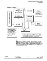
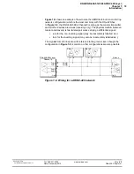
Figure 1-5. Receiver Diagram
Figure 1-5
is a block diagram of an ARINC receiver function. As illustrated,
received data may be placed directly into the 256-word FIFO by writing 0x0 in
the first label entry or may be passed through the label filter and the data change
filter before being accepted. Similarly, the parity checker and last data checker
can also be bypassed, if desired.
DNx ARINC-429 Receiver
ARINC-429 Receiver Hardware
Raw Frame
255 entry
Label Acceptance
Filter
Timestamp Source
Parity Error
Bit Checker
Data Change
Checker
RX FIFO
Trigger
Generator
“
Last Data
”
Memory
RX Frame Counter
(32-bit)
0x0 in the first entry
disables/bypasses filter.
entries skips them in
the verification/
acceptance process.
for the Scheduler.
Available only for
the RX0 receivers.
(256 x 32)
(256 x 32)
Counts one of the following: all frames accepted by the
label filter, parity error-free frames, frames placed into
verifies received
ARINC-429
frame against
“last data” value.
32-bit counter running
from sub-divider for
the 66 MHz clock,
shared across all RX
channels. Resolution
the FIFO, trigger initiator frames, or parity errors.
varies from 1 us to
1 second.
0x0 in subsequent


