2DA/2DB
2-2-1
5
6
1
9
11
10
3
8
7
13
4
2
12
14
15
;
Machine front
Machine inside
Machine rear
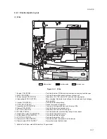
2-2-1 Electrical parts layout
(1) PCBs
Figure 2-2-1
PCBs
1. Engine PCB (EPCB) .................................... Controls the other PCBs, electrical components and optional devices.
2. Main PCB (MPCB) ....................................... Controls the operation panel and laser scanner unit.
3. Power source PCB (PSPCB) ....................... Gen24 V DC and 5V DC; controls the fixing heater.
4. High-voltage PCB (HVTPCB) ...................... Main charging. Generates high voltages for transfer and high voltages
for separation.
5. Inverter PCB (INPCB) .................................. Controls the exposure lamp.
6. CCD PCB (CCDPCB) .................................. Reads the image off originals.
7. Operation unit PCB (OPCB) ........................ Consists of the operation keys and display LEDs.
8. Drawer PCB (DPCB) ................................... Controls the electrical components.
9. APC PCB (APCPCB) ................................... Generates and controls the laser light.
10. PD PCB (PDPCB) ........................................ Controls horizontal synchronizing timing of laser beam.
11. Registration motor PCB (RMPCB) ............... Controls the registration motor.
12. Printer board PCB (PRNPCB) ..................... Controls the printer functions.
13. LCD PCB (LCDPCB) ................................... Controls the display of LCD.
14. Drawer main PCB (DMPCB)*
1 ............................
Controls electrical components of the drawer.
15. Drawer heater PCB (DHPCB)*
1 .........................
Relays the drawer heater power.
*1: Optional for 16 ppm model./Standard for 20 ppm model.
Summary of Contents for cd 1116
Page 1: ...Service Manual Copy CD 1116 CD 1120 Rev 1 ...
Page 2: ...Service Manual Copy DC 2116 DC 2120 Rev 1 ...
Page 4: ...This page is intentionally left blank ...
Page 247: ...2DA 2DB 1 2 3 2 Figure 2 3 2 Power source PCB silk screen diagram 220 240 V AC 120 V AC ...
Page 264: ...2DA 2DB 1 2 3 19 Figure 2 3 10 Operation unit PCB silk screen diagram ...


