background image

Technical Reference ________________________________________________________________

10 __________________________________________________________________ M210642EN-B

rising edge is synchronized to the GPS time. The duration of the high
state of the pulse is from 1 to 2 milliseconds. The 1PPS signal is
connected via D1 and buffer D2 to the system connector X1.

Programmable Logic Device

The programmable logic device (PLD) D1 is used to control the reset
function, the LED lamps, and the serial channel connections in the
unit.

The PLD is factory programmed via programming interface consisting
of signals TDI, TDO, TCK, and TMS.

The inverter gate D3-A is connected as oscillator and it supplies a
150 kHz clock signal for D1.

Serial Line Switch

The serial channel 1 from system connector (TXD1, RXD1) is
connected to the GPS module channel A (TXD1M, RXD1M) via
analog switch A2. The A2 consists of four separate switches, each
switch is controlled by PLD and a switch is closed if corresponding
control input G1, G2, G3 or G4 is at high level.

Switch 1 is used to connect the transmit signal TXD1M via buffer
amplifier A3-A to the serial line TXD1. Switch 2 and amplifier A3-B
are for possible future use.

Switch 3 is used to connect the TXD1 line signal to the line voltage
detector, which consists of transistors V1, V2, and diodes V3, V6. The
detector output at V1 collector is at high level if the line voltage is
below -3 V and the output is connected to the PLD for line switch
control.

Switch 4 is used to connect  the receive signal RXD1 to the GPS
module.

After power-up or reset switches 1, 2, 4 are open and switch 3 is
closed to allow the line voltage detector to monitor the TXD1 line.
According to the detector output the PLD logic determines the line
status as "idle" or "externally driven" at 200 ms intervals. The status is
'externally driven' if the line voltage was below -3 V for more than 5%

Summary of Contents for MRG112

Page 1: ...GPS Processor MRG112 TECHNICAL REFERENCE M210642EN B August 2005 ...

Page 2: ...mechanical including photocopying nor may its contents be communicated to a third party without prior written permission of the copyright holder The contents are subject to change without prior notice Please observe that this manual does not create any legally binding obligations for Vaisala towards the customer or end user All legally binding commitments and agreements are included exclusively in...

Page 3: ...fety Considerations 4 ESD Protection 4 Technical Support 5 CHAPTER 2 PRODUCT OVERVIEW 7 Introduction to GPS Processor MRG112 7 CHAPTER 3 FUNCTIONAL DESCRIPTION 9 GPS Module and Connections 9 Programmable Logic Device 10 Serial Line Switch 10 LED Lamp Operation 11 Reset Operation 12 Back up Power 12 CHAPTER 4 PARTS LIST 13 CHAPTER 5 DIAGRAMS AND BOARD LAYOUTS 15 CHAPTER 6 TECHNICAL DATA 19 Signal I...

Page 4: ...____________________________________ 2 ___________________________________________________________________ M210642EN B CONNECTOR SIGNAL LIST 23 APPENDIX C FRONT PANEL CONNECTORS 25 COM1 Connector 25 GPS ANT Connector 25 APPENDIX D LIST OF SIGNALS 27 ...

Page 5: ...his manual consists of the following chapters Chapter 1 General Information provides general notes for the product Chapter 2 Product Overview introduces the GPS Processor MRG112 features Chapter 3 Functional Description covers the connections and operation of MRG112 Chapter 4 Parts List contains a list of the MRG112 parts Chapter 5 Diagrams and Board Layouts lists the diagrams and board layouts Ch...

Page 6: ...Protection Electrostatic Discharge ESD can cause immediate or latent damage to electronic circuits Vaisala products are adequately protected against ESD for their intended use However it is possible to damage the product by delivering electrostatic discharges when touching removing or inserting any objects inside the equipment housing To make sure you are not delivering high static voltages yourse...

Page 7: ..._____ General Information VAISALA ________________________________________________________________________ 5 Technical Support For technical questions contact the Vaisala technical support E mail helpdesk vaisala com Phone int 358 9 8949 2789 Fax 358 9 8949 2790 ...

Page 8: ...Technical Reference ________________________________________________________________ 6 ___________________________________________________________________ M210642EN B This page intentionally left blank ...

Page 9: ...mmercial GPS Navigation Unit It is used for receiving satellite orbital data synchronizing with GPS time extracting local receiver position and velocity and for receiving local GPS signals to be used in the differential wind calculation The Base Unit is an E1 size card which contains system connector front plate and installation place and connectors for GPS Module The local antenna connector and t...

Page 10: ...Technical Reference ________________________________________________________________ 8 ___________________________________________________________________ M210642EN B This page intentionally left blank ...

Page 11: ...he same path The GPS module has two serial communication channels A and B The channel A is used for communication with the Control Processor and to send GPS data Channel A TXD1M RXD1M is connected to the system connector X1 via line switch A2 Channel B can be used to connect external data sources directly to the Module Channel B TXD2 RXD2M is connected to the front panel connector COM1 and to the ...

Page 12: ...M RXD1M via analog switch A2 The A2 consists of four separate switches each switch is controlled by PLD and a switch is closed if corresponding control input G1 G2 G3 or G4 is at high level Switch 1 is used to connect the transmit signal TXD1M via buffer amplifier A3 A to the serial line TXD1 Switch 2 and amplifier A3 B are for possible future use Switch 3 is used to connect the TXD1 line signal t...

Page 13: ...losed the left side pin connects corresponding operating voltage level to the pin with a current of up to 10 mA LED Lamp Operation The bicolor STATUS LED lamp V4 shows the status of MRG112 unit It is controlled by signals STLRED and STLGRN The lamp is red STLRED 0 green STLGRN 0 yellow STLRED 0 STLGRN 0 or dark both controls inactive During active reset V4 is yellow after reset the lamp is flashin...

Page 14: ...G112 is activated if either one input is active Back up Power The Module uses 5 V operating voltage and in addition the back up power VB is provided for the non volatile memory of the Module The back up power is supplied by a large capacitor C1 which is charged to approximately 4 2 V from 5 V operating voltage or from optional stand by voltage VSTBY via diodes V5 V10 and V11 The resistors R18 R20 ...

Page 15: ...43 GPS Receiver Module Assembly ref 7 26158 Hexagon Tapped Spacer Assembly ref 8 10948 Static Sensitive Sticker Assembly ref 9 15223 Serial No Sticker Table 2 Integrated Circuits Reference Part Number Description D1 25771 IC EPLD EPM7064STC44 10 D2 26570 IC Buffer Tiny NC7SZ125M5 D3 15964 IC Inverter 74HC14 SO14 A1 19483 IC Supervisor MAX810L A2 26119 IC Analog Switch MAX4512ESE A3 16730 IC Op Amp...

Page 16: ...8524 Cap Chip Ceramic 1n 5 NPO 50V 0805 C2 4 6 7 19941 Cap Chip Ceramic 100n 10 X7R 16V 0603 C8 25560 Cap Chip Tantalum 100uF 16V 20 Case E C1 18269 Cap Electolytic 1F 5 5V DB5R5D105 Table 6 Connectors Reference Part Number Description TP1 TP2 0172 Connector Pin E 309 6 X1 210249 Connector 2 mm Metric Ermet104732 X2 25056 Connector D DEJK9P4 1A7N X3 26106 Connector Socket HLE 115 02 G DV X4 18323 ...

Page 17: ...__________________________________________________________________ 15 CHAPTER 5 DIAGRAMS AND BOARD LAYOUTS This chapter lists the diagrams and board layouts Table 8 List of Diagrams Description Picture Code GPS Processor MRG112 Circuit Diagram DRW218338 GPS Processor MRG112 Components Layout DRW218395 ...

Page 18: ...Reference ________________________________________________________________ 16 __________________________________________________________________ M210642EN B 0409 017 Figure 1 GPS Processor MRG112 Circuit Diagram ...

Page 19: ..._______________________________________________ Diagrams and Board Layouts VAISALA _______________________________________________________________________ 17 0409 018 Figure 2 GPS Processor MRG112 Components Layout ...

Page 20: ...Technical Reference ________________________________________________________________ 18 __________________________________________________________________ M210642EN B This page intentionally left blank ...

Page 21: ...ications Signal Inputs GPS Receiver Module Type G12L Features Number of channels 12 Time to first fix 35 45 seconds warm cold Frequency 1575 MHz L1 band Signal level 130 50 dBm Connector SMA female at front panel LNA power 4 5 5 1 V 125 mA max RTCM input Data format RTCM 104 Data types 1 2 3 6 9 16 Signal levels RS232 Connector 9 pin male D at front panel Outputs Position and satellite information...

Page 22: ... V 5 500 mA 12 V 5 50 mA 12 V 5 50 mA Vstandby 3 30 V 5 mA max Operating conditions Temperature 5 55 ºC Humidity Non condensing Storage conditions Temperature 55 80 ºC Humidity Non condensing Dimensions and mass Unit type E1 size printed circuit board Length width height 190 128 20 6 mm Weight 265 g System connector Connector type 220 pin female LED Lamps Status indicator Bi color Led lamp SVs ind...

Page 23: ...__________________________________ Connector Signal Layout VAISALA _______________________________________________________________________ 21 APPENDIX A CONNECTOR SIGNAL LAYOUT System connector is a 220 pin 5 row female Connector ...

Page 24: ...___ M210642EN B Table 9 System Connector Signal Layout Pin Row a b c d e 1 GND GND GND GND GND 2 3 4 5 6 7 8 9 10 11 12 13 14 15 16 17 18 19 20 21 TXD2 22 RXD2B 23 GND GND GND GND GND 24 25 26 27 28 29 30 TXD1 31 RXD1 32 33 37 MRES 38 TDO TCK TDI TMS 39 1PPS 40 41 VSTBY 42 43 44 5 V 5 V 5 V 5 V 5 V 45 46 12 V 12 V GND 12 V 12 V 47 GND GND GND GND GND ...

Page 25: ...annel 2 RS232 TxD1 a30 Data output for serial channel 1 RS232 RxD1 a31 Data input for serial channel 1 RS232 MRES c37 Optional external reset input 3 3 V CMOS TDO A38 Data output in PLD programming 5 V CMOS TCK B39 Clock input in PLD programming 3 3 5 V CMOS TDI D39 Data input in PLD programming 3 3 5 V CMOS TMS E39 Mode select in PLD programming 3 3 5 V CMOS 1PPS a39 One pulse per second output 5...

Page 26: ...Technical Reference ________________________________________________________________ 24 __________________________________________________________________ M210642EN B This page intentionally left blank ...

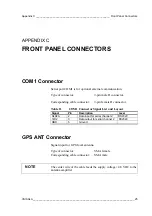
Page 27: ... connector 9 pin male D connector Corresponding cable connector 9 pin female D connector Table 11 COM1 Connector Signal List and Layout Signal Pin Description Level RxD2A 2 Data input for serial channel 2 RS232C TxD2 3 Data output for serial channel 2 RS232C GND 5 Ground GPS ANT Connector Signal input for GPS local antenna Type of connector SMA female Corresponding cable connector SMA male NOTE Th...

Page 28: ...Technical Reference ________________________________________________________________ 26 __________________________________________________________________ M210642EN B This page intentionally left blank ...

Page 29: ...Light emitting diode MHZ Megahertz MRES Master reset REDLED Red LED RXD1 Received serial line data 1 RXD1M Received serial data 1 to GPS Module RXD2A B Received serial data 2 A B RXD2M Received serial data 2 to GPS Module RXDA B Received serial data A B VSTBY Standby voltage STLGRN Status led green STLRED Status led red SVLGRN Satellite vehicle led green SVLRED Satellite vehicle led red TCK Test c...

Reviews: