


Service manual
6
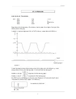
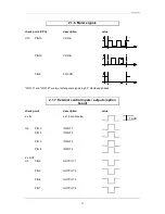
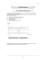
label photocell: reflection
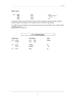
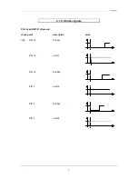
JP3:
PIN 1
VCC
5V
PIN 2
INP
see sketch
PIN 3
VSS
~ 2V
PIN 4
GND
0V
The voltage wave form at "INP" is similar to the one described under A ( measurable at U6 PIN4 too).
It has to be considered that the marking for the reflection photocell must be in a distance of 32,5 mm
to the interior rim, so that the photocell recognizes the marking.
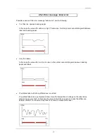
The "INP"-level can be displayed in the menu item "Parameter of the photocell" under "Reflection
photocell" (chapt. "2.5.4. Monitor"). The marking should have a size of at least 7 mm x 3 mm or bigger.


