


Service manual
5
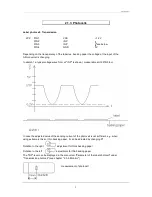
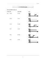
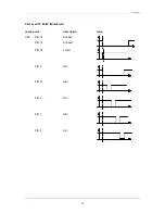
2.1.3. Photocells
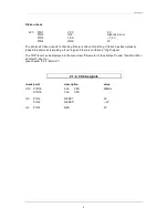
Label photocell: Transmission
JP2:
PIN 1
VSS
~1,2V
PIN 2
INP
PIN 3
INP
}
see below
PIN 4
GND
0V
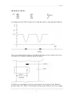
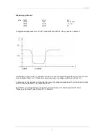
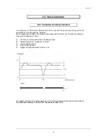
Depending on the transparency of the label res. backing paper the voltage at the input of the
AD-converter is changing.
In sketch 1 a typical voltage wave form at "INP" is shown ( measurable at U6 PIN3 too).
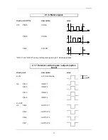
In case the adjusted value of the sending current of the photocell is not sufficient, e.g. when
using extremely thick or thin backing paper, it can be adjusted by changing P1.
Rotation to the right
adjustment for thick backing paper
Rotation to the left
adjustment for thin backing paper
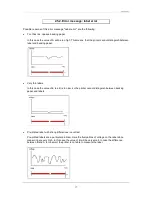
The "INP"-level can be displayed in the menu item "Parameter of the label photocell" under
"Transmission photocell" (see chapter "2.5.4. Monitor").
measurement of photocell


