FPGA Registers
EPU-4562 Programmer’s Reference Manual
18
SPI
C
ONTROL
R
EGISTERS
These are placed at the traditional offset 0x8 location. Only external SPX interface devices use
this interface. Because the board uses a 9-pin SPX connector, only two devices are supported.
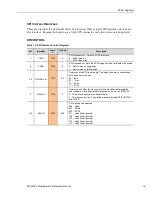
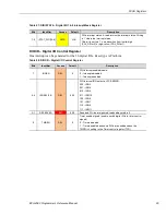
SPICONTROL
Table 13: SPI Interface Control Register
Bit
Identifier
Acces
s
Default
Description
7
CPOL
R/W
0
SPI clock polarity – Sets the SCLK idle state.
0
–
SCLK idles low
1
–
SCLK idles high
6
CPHA
R/W
0
SPI clock phase – Sets the SCLK edge on which valid data will be read.
0 – Data is read on rising edge
1 – Data is read on falling edge
5-4
SPILEN(1:0)
R/W
00
Determines the SPI frame length. This selection works in manual and
auto slave select modes.
00 – 8-bit
01 – 16-bit
10 – 24-bit
11 – 32-bit
3
MAN_SS
R/W
0
Determines whether the slave select lines are asserted through the
user software or are automatically asserted by a write to SPIDATA3.
0 - The slave select operates automatically
1 - The slave select line is controlled manually through SPICONTROL
bits SS[2:0]
2-0
SS(2:0)
R/W
000
SPI slave device selection:
000 – None
001 – SS0#
010 – SS1#
011 – Undefined (ignored)
100 – Undefined (ignored)
101 – Undefined (ignored)
110 – Undefined (ignored)
111 – Undefined (ignored)

