System Features
EBX-41 Reference Manual
25
S
ETTING THE
C
LOCK
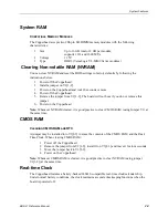
CMOS Setup (accessed by pressing the Delete key during a system boot) can be used to set the
time/date of the real-time clock.
Expansion Bus
PCI
E
/104
The PCIe/104 bus (connector J6) provides a PCIe x16 lane and two x1 lanes for add-on card
expansion. It supports both PCIe Gen1 and Gen2. Gen1 has a data rate of 2.5 GT/s and a
bandwidth of 250 MB/s. Gen2 has a data rate of 5.0 GT/s and a bandwidth of 500 MB/s. See the
PCI/104-Express & PCIe/104 Express Specification
for signal details.
SUMIT
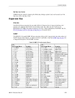
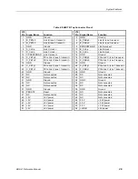
The SUMIT A Top and SUMIT B Top connectors (J14 and J10, respectively) provide a subset of
the PCI Express functionality, as shown in Table 5 and Table 6. See the
SUMIT Specification
for
a complete description of the SUMIT interface.
Table 5: SUMIT A Top Connector Pinout
J14
Pin
Signal Name
Function
J14
Pin
Signal Name
Function
1
+5VSB
+5V power
2
+12V
+12V power
3
3.3V
+3.3V power
4
SMB/I2C_DATA
SMBus data
5
3.3V
+3.3V power
6
SMB/I2C_CLK
SMBus clock
7
NC
Not connected
8
SMB/I2C_ALERT#
SMBus interrupt line in
9
NC
Not connected
10
SPI/uWire_DO
SPI data out from master
11
NC
Not connected
12
SPI/uWire_DI
SPI data in to master
13
NC
Not connected
14
SPI/uWire_CLK
SPI clock
15
+5V
+5V power
16
SPI/uWire_CS0#
SPI chip select 0
17
USB3+
USB3 data +
18
SPI/uWire_CS1#
SPI chip select 1
19
USB3-
USB3 data
–
20
NC
Not connected
21
+5V
+5V power
22
NC
Not connected
23
USB2+
USB2 data +
24
LPC_AD0
LPC line 0
25
USB2-
USB2 data
–
26
LPC_AD1
LPC line 1
27
+5V
+5V power
28
LPC_AD2
LPC line 2
29
USB1+
USB1 data +
30
LPC_AD3
LPC line 3
31
USB1-
USB1 data
–
32
LPC_FRAME#
LPC frame
33
+5V
+5V power
34
SERIRQ#
Serial IRQ legacy
35
USB0+
USB0 data +
36
NC
Not connected
37
USB0-
USB0 data
–
38
CLK_33MHz
33 MHz clock out
39
GND
Ground
40
GND
Ground
41
A_PETp0
Link A, lane 0 tr
42
A_PERp0
Link A, lane 0 r
43
A_PETn0
Link A, lane 0 transmit
–
44
A_PERn0
Link A, lane 0 receive
–
45
GND
Ground
46
APRSNT#/GND
Link A card present
47
PERST#
Reset
48
A_CLKp
Link A clock +
49
WAKE#
Wake on event signal
50
A_CLKn
Link A clock
–
51
+5V
+5V power
52
GND
Ground


