System Features
EBX-41 Reference Manual
26
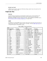
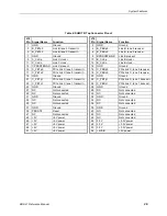
Table 6: SUMIT B Top Connector Pinout
J10
Pin
Signal Name
Function
J10
Pin
Signal Name
Function
1
GND
Ground
2
GND
Ground
3
B_PETp0
Link B, lane 0 tr
4
B_PERp0
Link B, lane 0 r
5
B_PETn0
Link B, lane 0 transmit
–
6
B_PERn0
Link B, lane 0 receive
–
7
GND
Ground
8
BPRSNT#/GND
Link B present
9
C_CLKp
Link C clock +
10
B_CLKp
Link B clock +
11
C_CLKn
Link C clock
–
12
B_CLKn
Link B clock
–
13
CPRSNT#/GND Link C present
14
GND
Ground
15
C_PETp0
PCIe link C, lane 0 tr
16
C_PERp0
PCIe link C, lane 0 r
17
C_PETn0
PCIe link C, lane 0 transmit
– 18 C_PERn0
PCIe link C, lane 0 receive
–
19
GND
Ground
20
GND
Ground
21
C_PETp1
PCIe link C, lane 1 tr
22
C_PRTp1
PCIe link C, lane 1 tr
23
C_PETn1
PCIe link C, lane 1 transmit
– 24 C_PERn1
PCIe link C, lane 1 transmit
–
25
GND
Ground
26
GND
Ground
27
NC
Not connected
28
NC
Not connected
29
NC
Not connected
30
NC
Not connected
31
GND
Ground
32
GND
Ground
33
NC
Not connected
34
NC
Not connected
35
NC
Not connected
36
NC
Not connected
37
GND
Ground
38
GND
Ground
39
PERST#
Reset
40
NC
Not connected
41
NC
Not connected
42
NC
Not connected
43
+5V
+5V power
44
NC
Not connected
45
+5V
+5V power
46
3.3V
+3.3V power
47
+5V
+5V power
48
3.3V
+3.3V power
49
+5V
+5V power
50
3.3V
+3.3V power
51
+5V
+5V power
52
+5VSB
+5V power


