background image


Physical Dimensions 

EPM-4 Reference Manual 

    R

eference

 – 

19 

H

ARDWARE 

A

SSEMBLY


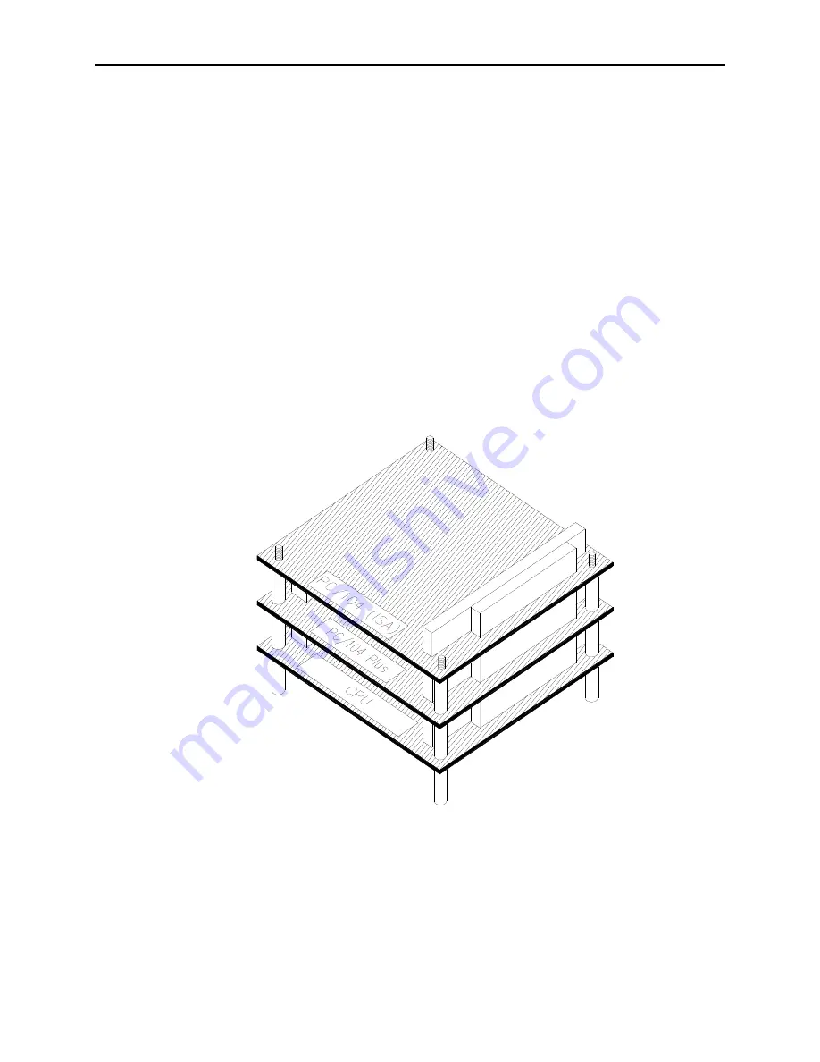
The EPM-4 uses pass-through PC/104 and PC/104-

Plus

 connectors so that expansion modules 

can be added to the top or bottom of the stack. PC/104 (ISA) modules must NOT be positioned 
between the Lynx and any PC/104-

Plus 

(PCI) modules on the stack. The PC/104 pass-through 

connector on the EPM-4 Rev 4 is keyed (pins B10 and C19 missing) to provide greater 
compatibility with other PC/104 compliant devices.  

The entire assembly can sit on a tabletop or it can be secured to a base plate. When bolting the 
unit down, make sure to secure all four standoffs to the mounting surface to prevent circuit board 
flexing. Standoffs are secured to the top circuit board using four pan head screws. Refer to the 
drawing on page 17 for dimensional details. 

An extractor tool is available (part number VL-HDW-201) to separate the modules from the 
stack. 

S

TACK 

A

RRANGEMENT


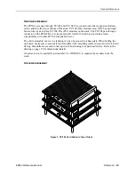
Figure 3. PC/104 Card Added to Top of Stack 

Summary of Contents for EPM-4

Page 1: ...Reference Manual DOC REV 3 16 2009 EPM 4 Lynx AMD ÉlanSC520 processor module with 10 100 Ethernet and PC 104 Plus interface ...

Page 2: ...EPM 4 AMD ÉlanSC520 processor module with 10 100 Ethernet and PC 104 Plus interface MEPM4 ...

Page 3: ...same protection value 3 0V battery Rev 3 Release EPM 4g model release Initial RoHS version Rev 2 Release Initial public release Support Page The EPM 4 Support Page at http www VersaLogic com private lynxsupport asp contains additional information and resources for this product including Reference Manual PDF format Operating system information and software drivers Data sheets and manufacturers link...

Page 4: ...gh every effort has been made to ensure this document is error free VersaLogic makes no representations or warranties with respect to this product and specifically disclaims any implied warranties of merchantability or fitness for any particular purpose VersaLogic reserves the right to revise this product and associated documentation at any time without obligation to notify anyone of such changes ...

Page 5: ......

Page 6: ...S Setup IDE Configuration 11 IDE 11 IDE setup 11 CMOS Setup Advanced Configuration 12 D0000h 64k page function 12 PLD register base I O 12 Force Ethernet 10 BaseT 12 PS 2 Mouse IRQ12 13 LPT1 0378h 13 Parallel Port Mode 13 CPU Speed 13 Cache Mode 13 Write Buffer 13 GP Bus Timings 13 COM1 03F8h RS 232 14 COM2 02F8h RS 232 14 COM3 03E8h RS 422 485 14 COM4 02E8h RS 422 485 14 GP Timer 0 GP Timer 1 Wat...

Page 7: ... ROM Interface 28 Utility Connector J7 29 Keyboard Mouse Interface 30 Programmable LED 30 External Speaker 30 Push Button Reset 30 General Purpose Timer Inputs 30 Parallel Floppy Port 31 Parallel Port Operation 31 Floppy Port Operation 31 Parallel Floppy Port Pinout 31 Ethernet Interface 32 BIOS Configuration 32 Status LED 32 Ethernet Connector 32 Watchdog Timer 33 Expansion Bus 34 PC 104 Plus PCI...

Page 8: ...Table of Contents v Appendix B References 45 ...

Page 9: ...s operation possible Extended temperature options 100MHz Transient Voltage Suppressor Devices RoHS compliant version available The EPM 4 is a complete computer system in one board It may be used alone or with expansion modules It features a PC 104 Plus expansion interface for fast PCI based interface to a wide variety of PC 104 and PC 104 Plus stacking modules This card is designed to be used prim...

Page 10: ...ompactFlash socket LPT Floppy Interface Supports one floppy drive or parallel port Ethernet Interface Autodetect 10BaseT 100BaseTX based on Intel 82551ER 12K transmit receive buffer COM1 and COM2 Interface RS 232 16C550 compatible 115K baud max COM3 and COM4 Interface RS 422 485 16C550 compatible 460K baud max Connectors Utility 2mm 50 pin shrouded IDE 2mm 44 pin Floppy LPT 2mm 20 pin shrouded Eth...

Page 11: ...EPM 4 Block Diagram EPM 4 Reference Manual Introduction 3 EPM 4 Block Diagram ...

Page 12: ...mium hexavalent chromium and the presence of polybrominated biphenyls PBB and polybrominated diphenyl ethers PBDE flame retardants in certain electrical and electronic products sold in the European Union EU beginning July 1 2006 VersaLogic Corporation is committed to supporting customers with high quality products and services meeting the European Union s RoHS directive ROHS COMPLIANT CABLES Adapt...

Page 13: ... we have questions Quantity of items being returned The model and serial number bar code of each item A description of the problem Steps you have taken to resolve or repeat the problem The return shipping address Warranty Repair All parts and labor charges are covered including return shipping charges for UPS Ground delivery to United States addresses Non warranty Repair All non warranty repairs a...

Page 14: ......

Page 15: ...static free surface component side up Use an anti static foam pad if available The board should also be protected during shipment or storage by keeping inside a closed metallic anti static envelope Note The exterior coating on some metallic anti static bags is sufficiently conductive to cause excessive battery drain if the bag comes in contact with the bottom side of the EPM 4 LITHIUM BATTERY Warn...

Page 16: ...figuration and Setup The following list describes the components recommended for setting up a typical development system RECOMMENDED COMPONENTS EPM 4 Board and cable kit ATX Power Supply EPM VID 3 for video support Keyboard with PS 2 connector mouse Ethernet Network IDE Hard Drive Floppy Drive ...

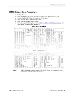
Page 17: ...mory Test Tick Enabled Drive H None Boot 4th None Debug Breakpoints Unused Drive I None Boot 5th None Debugger Hex Case Upper Drive J None Boot 6th None Memory Test StdLo FastHi Drive K None Loader Unused ATA DRV ASSIGNMENT Sect Hds Cyls Memory Ide 0 3 AUTOCONFIG LBA Base FLOPPY DRIVE TYPES Ide 1 3 AUTOCONFIG LBA 633KB Floppy 0 1 44 MB 3 5 Ide 2 Not installed Ext Floppy 1 Not installed Ide 3 Not i...

Page 18: ... enter CMOS Setup the BIOS ignores DEL from a PS 2 keyboard This is normal operation of the Lynx COM2 is configured for standard serial port communication 9600 Baud Parity None Flow Control None Data Bits 8 Stop Bits 1 Console redirection remains active when POST completes and the operating system boots Text based operating systems such as DOS and Linux can be controlled over this connection To en...

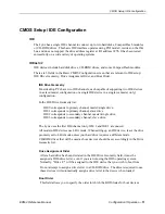
Page 19: ...e Geometry list IDE 0 corresponds to primary channel master single drive IDE 1 corresponds to primary channel slave drive IDE 2 corresponds to secondary channel master single drive IDE 3 corresponds to secondary channel slave drive The Lynx uses the first IDE channel only IDE 2 and IDE 3 are unused All modern IDE devices use LBA mode When setting up an IDE device leave the drive geometry set to LB...

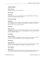
Page 20: ...e flash chip which may contain 3rd party Ethernet boot code or any other BIOS extension not included If there is a such an extension present it will be called by the BIOS The BIOS extension can be programmed into the flash chip with the FBU utility For remote booting via Ethernet the recommended boot ROM is Managed PC Boot Agent from Argon Technology Corporation RAM System RAM is exposed in the D0...

Page 21: ... maximum clock rate for the ÉlanSC520 Microcontroller is 133 MHz It can optionally be set to 100 MHz for a slight power savings If an extended temperature board version is detected the default will change to 100 MHz CACHE MODE Default Write Back The 16 kb L1 cache can be configured for either write through or write back mode This option controls the CACHE_WR_MODE in the CPUCTL register MMCR offset...

Page 22: ...sabled the IRQ and I O space are freed COM4 02E8H RS 422 485 Default Disabled Allows you to disable or specify the IRQ used by UART2 on the SMSC FDC37B727 Super I O When disabled the IRQ and I O space are freed GP TIMER 0 GP TIMER 1 WATCHDOG TIMER Default Disabled These internal SC520 devices can be disabled or enabled by assigning an IRQ Enabling these devices only sets up the IRQ assignment it i...

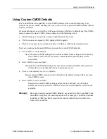
Page 23: ...efaults Saves the current CMOS settings to the custom defaults These settings will be used any time CMOS is reset If there are already custom defaults specified they will be overwritten Reset CMOS to custom defaults Discards the current CMOS settings and uses the saved custom defaults This operation will fail if no custom defaults have been previously saved Clear custom defaults use factory defaul...

Page 24: ......

Page 25: ... complies with all PC 104 Plus standards Dimensions are given below to help with pre production planning and layout Figure 1 Dimensions Not to scale All dimensions in inches 3 2 330 3 070 3 575 3 370 0 400 0 000 0 200 3 300 0 150 3 050 3 470 3 570 3 350 3 150 0 000 0 200 0 250 ...

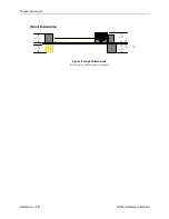
Page 26: ...Physical Dimensions Reference 18 EPM 4 Reference Manual HEIGHT DIMENSIONS Figure 2 Height Dimensions Not to scale All dimensions in inches 0 44 0 42 0 51 0 44 0 06 ...

Page 27: ...ins B10 and C19 missing to provide greater compatibility with other PC 104 compliant devices The entire assembly can sit on a tabletop or it can be secured to a base plate When bolting the unit down make sure to secure all four standoffs to the mounting surface to prevent circuit board flexing Standoffs are secured to the top circuit board using four pan head screws Refer to the drawing on page 17...

Page 28: ...ugh PC 104 ISA connector is keyed pins B10 and C19 missing for greater compatibility with PC 104 devices as shown in the figure below Figure 5 PC 104 ISA Connector Keying C19 B10 B1 A1 B32 A32 Pin numbering begins on the side with a larger row offset C19 D19 C0 D0 Note For rows A and B pin numbers begin at 1 For rows C and D pin numbers begin at 0 Pin Side of ISA Connector ...

Page 29: ...g Connector Transition Cable Cable Description Page Pin 1 Location X Coord Y Coord J1 PC 104 Plus AMP 1375799 1 __ __ 34 450 3 139 J2 LPT Floppy FCI 89947 720 DB 25 to floppy CBL CBR 2003 CBL CBR 2501 12 2mm latching LPT Floppy adapter cable 31 0 071 2 465 J3 PLD Reprogramming Port Factory use Only __ __ __ __ 450 2 525 J4 Ethernet RJ45 __ __ 32 3 935 2 545 J5 CompactFlash Type I II __ __ __ 28 __...

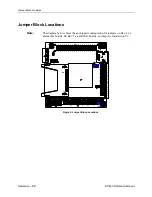
Page 30: ... EPM 4 Reference Manual Jumper Block Locations Note The diagram below shows the as shipped configuration for jumpers on Rev 4 xx and earlier boards On Rev 5 xx and later boards no jumper is installed on V3 Figure 6 Jumper Block Locations ...

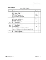
Page 31: ...ediate 5 6 Out and 7 8 In RS 422 5 6 In 7 8 In 27 V3 Rev 4 xx and earlier CompactFlash Master Slave Section In Master IDE Device Out Slave IDE Device In 28 V3 Rev 5 xx and later CompactFlash Master Slave Section In Slave IDE Device Out Master IDE Device Out 28 V4 1 2 System BIOS Selector In Run Time System BIOS occupies E0000h to FFFFFh Out Master System BIOS occupies E0000h to FFFFFh Note The Run...

Page 32: ...tor on the crimp housing that corresponds to pin 10 of the pinout Table 3 Main Power Connector Pinout J8 Pin Signal Name Description 1 Ground Ground 2 5VDC Power Input 3 Ground Ground 4 12VDC Power Input 5 Ground Ground 6 12VDC Power Input 7 3 3VDC Power Input 8 5VDC Power Input 9 Ground Ground 10 5VDC Power Input Note The 3 3VDC 12VDC and 12VDC inputs are only required for expansion modules that ...

Page 33: ... speed from 133 MHz to 100 MHz via the BIOS settings will save approximately 0 5 W LITHIUM BATTERY Warning To prevent shorting premature failure or damage to the lithium battery do not place the unit on a conductive surface such as metal black conductive foam or the outside surface of a metalized ESD protective pouch The lithium battery may explode if mistreated Do not recharge disassemble or disp...

Page 34: ... back to position 2 3 for normal operation Note Operation of the board with jumper V1 in the erase position 1 2 is not supported or recommended DEFAULT CMOS RAM SETUP VALUES After the CMOS RAM is cleared the system will load default CMOS RAM parameters the next time the board is powered on The default CMOS RAM setup values will be used in order to boot the system whenever the main CMOS RAM values ...

Page 35: ...o 460K baud Interrupt assignment for each COM port is handled in CMOS Setup and each port can be independently enabled or disabled All four serial ports are protected against ESD damage This protection exceeds 15KV human body model COM PORT CONFIGURATION There are no configuration jumpers for COM1 and COM2 because it only operates in RS 232 mode Jumper V2 is used to configure COM3 and COM4 for RS ...

Page 36: ...from CPU 2 Ground Ground Ground 3 IDE7 DATA 7 Data bit 7 4 ID8 DATA 8 Data bit 8 5 ID6 DATA 6 Data bit 6 6 ID9 DATA 9 Data bit 9 7 ID5 DATA 5 Data bit 5 8 ID10 DATA 10 Data bit 10 9 ID4 DATA 4 Data bit 4 10 ID11 DATA 11 Data bit 11 11 ID3 DATA 3 Data bit 3 12 ID12 DATA 12 Data bit 12 13 ID2 DATA 2 Data bit 2 14 ID13 DATA 13 Data bit 13 15 ID1 DATA 1 Data bit 1 16 ID14 DATA 14 Data bit 14 17 ID0 DA...

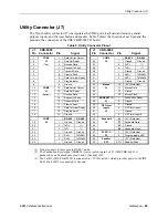
Page 37: ...etect 34 J4 T1 Mouse Data 11 J3 15 Data Set Ready 35 T3 Ground 12 Bottom 11 Receive Data 36 T5 Mouse Clock 13 16 Request to Send 37 PBRESET 2 1 Pushbutton Reset 14 12 Transmit Data 38 S1 2 Ground 15 17 Clear to Send 39 GP Timer 3 Ground 16 13 Data Terminal Ready 40 Inputs 4 GP Timer Input 1 17 18 Ring Indicator 41 J2 Ground 18 14 Ground 42 5 GP Timer Input 0 COM3 RS 422 RS 485 43 Keyboard B4 5V Pr...

Page 38: ...e MMCR base address defaults to DF00 0 segment offset address The external LED is duplicated with an on board LED The green LED in D5 See page 22 is also controlled by the PIO24 pin Note The LED is turned on by the BIOS during system startup This causes the light to function as a power on indicator if it is not otherwise controlled by user code EXTERNAL SPEAKER A miniature 8 ohm speaker can be con...

Page 39: ... and connect a floppy disk drive to the parallel port cable CBL CBR 2003 using the floppy disk cable CBL CBR 2501 The diagram below shows how to connect the drive PARALLEL FLOPPY PORT PINOUT Table 6 LPT1 Parallel Floppy Port Pinout J2 Pin Centronics Signal Floppy Signal Signal Direction 1 Strobe DS0 Out 2 Auto feed RPM Out 3 Data bit 1 INDEX In Out 4 Printer error HDSEL In 5 Data bit 2 TRK0 In Out...

Page 40: ...Activity ON Active Ethernet cable plugged into J4 No Tx Rx data activity OFF Cable not plugged into J4 Cable not plugged into active hub BLINKING Active Ethernet cable plugged into J4 Tx or Rx data activity detected on the cable Yellow LED Speed ON 100baseTx Fast detected on Ethernet cable OFF 10BaseTx Slow detected on Ethernet cable ETHERNET CONNECTOR A board mounted RJ 45 connector is provided t...

Page 41: ...MCR_base 0CB0h MemWrite WDTMRCTL 03333h Key sequence to allow write access to control MemWrite WDTMRCTL 0CCCCh register These are 16 bit memory writes MemWrite WDTMRCTL 0C010h Enable watchdog timer 4 second timer Reset on timeout Begin program loop perform useful instructions here that will never take more than 4 seconds to complete MemWrite WDTMRCTL 0AAAAh Key sequence to reset the timer countdow...

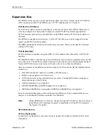
Page 42: ...mented as the ISA bus on the Lynx The GP bus is similar in function to the ISA bus but not functionally identical Nearly all PC 104 devices in use today will work on the Lynx without modification Here is a summary of the differences between a legacy ISA bus and the GP bus implementation on the Lynx Only DMA channels 5 and 6 are available to PC 104 devices IRQ15 is not available to PC 104 devices P...

Page 43: ... 35 PC 104 Modules PC 104 I O modules should be addressed in the 104h 3FFh address range Care must be taken to avoid the I O addresses shown in the On Board I O Devices table on page 37 These ports are used by on board peripherals and video devices ...

Page 44: ... DF000h through DFFFFh will instead by occupied by the MMCR For this reason the maximum BIOS extension size is reduced from 64KB to 60KB In the event of an address conflict the MMCR base address can be moved at any time with an I O write to the Configuration Base Address Register CBAR located at I O address FFFCh Refer to the ÉlanSC520 Register Set Manual for further details MEMORY MAP The lower 1...

Page 45: ...Devices I O Device Standard I O Addresses See ÉlanSC520 register set manual 000h 0FFh Special Control Register 0E0h Revision Indicator Register 0E1h Map and Paging Control Register 0E3h Primary IDE Controller 1F0h 1F6h COM 4 Serial Port 2E8h 2EFh COM 2 Serial Port 2F8h 2FFh COM 3 Serial Port 3E8h 3EFh Floppy Disk Controller 3F0h 3F7h COM1 Serial Port 3F8h 3FFh CBAR FFFCh FFFFh Note I O ports occup...

Page 46: ... the Lynx Not all devices can use all IRQ s Refer to Figure 8 for a description of allowable IRQ assignments for each device Figure 8 Interrupt Circuit Diagram Components Group COM1 COM2 GP Timers Watchdog PCI Interrupts COM3 COM4 LPT1 Available on PC 104 ISA bus Default IRQ assignments 0 Timer 0 1 Keyboard 2 Slave PIC cascade 3 COM2 4 COM1 5 Unused 6 Floppy drive 7 Unused 8 Real Time Clock 9 Unus...

Page 47: ...s Bit Mnemonic Description D7 D6 Reserved These bits have no function D5 SB SEL BIOS Selector Input Indicates the status of jumper V4 1 2 SB SEL 0 Jumper V4 1 2 Out Master BIOS SB SEL 1 Jumper V4 1 2 In Run Time BIOS Note This general purpose bit is read only D4 D1 Reserved These bits have no function D0 GPI General Purpose Input Indicates the status of TTL input GPI 0 Jumper V4 3 4 Out GPI 1 Jump...

Page 48: ...EPM 4 will always read as 11011 Other codes are reserved for future products PC4 PC3 PC2 PC1 PC0 Product Code 1 1 0 1 1 EPM 4 Note These bits are read only D2 D1 REV1 REV0 Revision Level These bits are represent the EPM 4 circuit revision level REV1 REV0 Revision Level 0 0 Current product release 0 1 Reserved 1 0 Reserved 1 1 Reserved Note These bits are read only D0 ET Extended Temperature This b...

Page 49: ...emory FPGEN 0 FLASH page frame disabled FPGEN 1 FLASH page frame enabled Note When FPGEN 1 the Page Select bits are used to access various blocks within the FLASH The D0000h 64k page function in CMOS Setup must be set to ISA Bus D6 D3 Reserved These bits have no function D2 D0 PG2 PG0 Page Select Selects which 64K block of FLASH will be mapped into the page frame Memory Range within PG2 PG1 PG0 FL...

Page 50: ......

Page 51: ...ed Red J1 High Density Connector FCI 98414 F06 50U 2mm 50 pins keyed latching header J2 Timer and Reset input Conta Clip 10250 4 5 pin screw terminal J3 COM1 COM2 Kycon K42 E9P P A4N Dual stacked DB 9 male J4 PS 2 Keyboard and Mouse Kycon KMDG 6S 6S S4N Dual stacked PS 2 female J5 COM4 Conta Clip 10250 4 5 pin screw terminal J6 COM3 Conta Clip 10250 4 5 pin screw terminal R1 Resistor DigiKey P332C...

Page 52: ...XRI1 XRXD2 XDCD2 XCTS1 XRTS1 XDTR2 XTXD2 GRN OR D1 LED 1 3 2 4 MTH4 1 1 MTH2 1 1 MTH1 1 1 MKPWR SPKO SP1 SPEAKER S1 3 2 1 PBRST PLED MKPWR XDSR2 XDCD1 XDTR1 XRI2 XCTS2 XRTS2 TX3 TRX4 TX4 XRXD1 XTXD1 TRX3 XTXD2 XDTR2 XRXD2 XDCD2 COM4 TRX3 TX3 TRX4 TX4 COM3 XRI1 XRTS1 XDSR1 XCTS1 COM1 COM2 TMRIN1 TMRIN0 KBC5 KBD1 MSC5 MSD1 J6 JTB251 01 05 1 1 2 2 3 3 4 4 5 5 J5 JTB251 01 05 1 1 2 2 3 3 4 4 5 5 J2 JT...

Page 53: ...ration www intel com design 82551ER PC 104 Specification PC 104 Consortium www pc104 org PC 104 Resource Guide PC 104 Plus Specification PC 104 Consortium www pc104 org PC 104 Resource Guide General PC Documentation Microsoft Press www microsoft com learning books The Programmer s PC Sourcebook General PC Documentation Powell s Books www powells com The Undocumented PC B ...

Reviews: