Operation
VL-EPMs-U1 Reference Manual
23
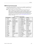
SUMIT-A Top Connector (J6)
The table below shows the SUMIT-A Top connections to the VL-EPMs-U1. Signals that are not
connected are pass-through only. The +5V signals on this connector are available to power the
VL-EPMs-U1. This connector is present on all models.
Note:
SUMIT technology uses an automatic link alignment feature (also known as “lane
shifting”) to eliminate the need for jumpers or switches to identify an expansion
module’s position in the stack. Signals are not simply passed straight up from the bottom
connector to the top on SUMIT modules. Links that are used by the expansion module
are automatically selected, and the remaining unused signals are shifted down to the
consumed link’s pins on the top connector for use by the next board. Both PCIe and USB
signals are subject to auto-alignment. See
page 28 of the SUMIT Specification
for an
explanation of this feature.
Table 10: SUMIT-A Top Connector Pinout
Pin Signal Name
Function
Pin Signal Name
Function
1
+5V
SB
+5V power standby
2
+12V
+12V power
3
+3.3V
+3.3V power
4
SMB/I2C_DATA
SMBus data
5
+3.3V
+3.3V power
6
SMB/I2C_CLK
SMBus clock
7
EXPCD_REQ#
ExpressCard request
8
SMB/I2C_ALERT#
SMBus interrupt line in
9
EXPCD_PRSNT#
ExpressCard present
10
SPI/µWire_DO
SPI data out from master
11
USB_OC#
USB overcurrent flag
12
SPI/µWire_DI
SPI data in to master
13
Reserved
Pass-through
14
SPI/µWire_CLK
SPI clock
15
Reserved
Pass-through
16
SPI/µWire_CS0#
SPI chip select 0
17
Reserved
Pass-through
18
SPI/µWire_CS1#
SPI chip select 1
19
Reserved
Pass-through
20
Reserved
Pass-through
21
+5V
+5V power
22
Reserved
Pass-through
23
USB2+
USB2 data +
24
LPC_AD0
LPC line 0
25
USB2-
USB2 data
–
26
LPC_AD1
LPC line 1
27
+5V
+5V power
28
LPC_AD2
LPC line 2
29
USB1+
USB1 data +
30
LPC_AD3
LPC line 3
31
USB1-
USB1 data
–
32
LPC_FRAME#
LPC frame
33
+5V
+5V power
34
SERIRQ#
Serial IRQ legacy
35
USB0+
USB0 data +
36
LPC_PRSNT#/GND LPC card present
37
USB0-
USB0 data
–
38
CLK_33MHz
33 MHz clock out
39
GND
Ground
40
GND
Ground
41
A_PETp0
Link A, lane 0 tr
42
A_PERp0
Link A, lane 0 r
43
A_PETn0
Link A, lane 0 transmit
–
44
A_PERn0
Link A, lane 0 receive
–
45
GND
Ground
46
APRSNT#/GND
Link A card present
47
PERST#
Reset
48
A_CLKp
Link A clock +
49
WAKE#
Wake
50
A_CLKn
Link A clock
–
51
+5V
+5V power
52
GND
Ground


