Operation
VL-EPMs-U1 Reference Manual
26
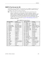
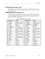
SUMIT-A Bottom Connector (J12)
The table below shows the SUMIT-A Bottom connections to the VL-EPMs-U1. Signals that are
not connected are pass-through only. The +5V and ground signals on this connector are available
to power the VL-EPMs-U1. This connector is present on all models. (See the SUMIT "lane
shifting" note on page 23.)
Table 13: SUMIT-A Bottom Connector Pinout
Pin Signal Name
Function
Pin Signal Name
Function
1
+5V
SB
+5V power standby
2
+12V
+12V power
3
+3.3V
+3.3V power
4
SMB/I2C_DATA
SMBus data
5
+3.3V
+3.3V power
6
SMB/I2C_CLK
SMBus clock
7
EXPCD_REQ#
ExpressCard request
8
SMB/I2C_ALERT#
SMBus interrupt line in
9
EXPCD_PRSNT#
ExpressCard present
10
SPI/uWire_DO
SPI data out from master
11
USB_OC#0/1
USB0-1 overcurrent flag
12
SPI/uWire_DI
SPI data in to master
13
Reserved
Pass-through
14
SPI/uWire_CLK
SPI clock
15
Reserved
Pass-through
16
SPI/uWire_CS0#
SPI chip select 0
17
Reserved
Pass-through
18
SPI/uWire_CS1#
SPI chip select 1
19
Reserved
Pass-through
20
Reserved
Pass-through
21
+5V
+5V power
22
Reserved
Pass-through
23
USB2+
USB2 data +
24
LPC_AD0
LPC line 0
25
USB2-
USB2 data
–
26
LPC_AD1
LPC line 1
27
+5V
+5V power
28
LPC_AD2
LPC line 2
29
USB1+
USB1 data +
30
LPC_AD3
LPC line 3
31
USB1-
USB1 data
–
32
LPC_FRAME#
LPC frame
33
+5V
+5V power
34
SERIRQ#
Serial IRQ legacy
35
USB0+
USB0 data +
36
LPC_PRSNT#/GND LPC card present
37
USB0-
USB0 data
–
38
CLK_33MHz
33 MHz clock out
39
GND
Ground
40
GND
Ground
41
A_PETp0
Link A, lane 0 tr
42
A_PERp0
Link A, lane 0 r
43
A_PETn0
Link A, lane 0 transmit
–
44
A_PERn0
Link A, lane 0 receive
–
45
GND
Ground
46
APRSNT#/GND
Link A card present
47
PERST#
Reset
48
A_CLKp
Link A clock +
49
WAKE#
Wake
50
A_CLKn
Link A clock
–
51
+5V
+5V power
52
GND
Ground


