3
DSUB 9-pin Accessory Connector
Pin 1
: Output Logic squelch
High: Radio receiving the signal with the correct CTCSS or DCS.
Low: Radio not receiving the signal with the correct CTCSS or DCS.
Pin 2
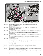
: Output Rx discriminator (Need to set the solder short on the PCB)
JP3 (JP1503) - Flat: 10 Hz to 3.0 kHz (140 mVrms / STD deviation with 600 ohm termination)
or
JP4 (JP1504) - Filtered 300 Hz to 3.0 kHz (70 mVrms / STD deviation with 600 ohm termination)
* JP3: Closed from the factory.
JP4: Not closed from the factory.
Pin 3
: Input TX data to the radio modulator. (Flat: 10 Hz to 3.0 kHz)
(40 mVrms / STD deviation)
Pin 4
: DTR / TXD: Not used
Pin 5
: Ground
Pin 6
: Output Horn alert signal (Open collector with maximum 16.0 V, 100 mA sink).
Pin 7
: Input external PTT
[Low: Request the transmission]
[High: Request the Receiving]
Pin 8
: Output supply voltage (Need to set the solder short on the PCB)
JP1 (JP1501) Output 5.0 V (Maximum 100 mA output)
or
JP2(JP1502) Output 13.2 V (Maximum 100 mA output)
* Both JP1 and JP2 are not closed from the factory.
Pin 9
: Input the ignition signal of the CAR.
This signal is for the following operation,
(1) Disable the Horn alert during the ignition is turned on.
(2) Turn on and off the radio. This function requires the solder short JP8 (JP1508).
Summary of Contents for VX-2500EV
Page 5: ...5 Block Diagram 1 ...
Page 6: ...6 Block Diagram 2 ...
Page 7: ...7 Interconnection Diagram ...
Page 8: ...8 Note ...
Page 18: ...18 RF Unit Jumper Information Note ...
Page 34: ...PANEL Unit 34 Note ...
Page 43: ...19 ...


