9
Circuit Description
1. Overview
The
VX-2500EV
is a UHF FM mobile transceiver designed
to operate in the frequency range of 134 to 174MHz.
2. Circuit Configuration by Frequency
The receiver is a double-conversion superheterodyne with
a first intermediate frequency(IF) of 44.25MHz and a sec-
ond IF of 450kHz. Incoming signals from the antenna are
mixed with the local signal from PLL to produce the first
IF of 44.25MHz.
This is then mixed with the 44.25MHz second local os-
cillator (using the 14.6MHz reference TCXO) output to
produce the 450kHz second IF. This is detected to give
the demodulated signal.
The transmit signal frequency is generated by PLL VCO,
and modulated by the signal from the microphone. It is
then amplified and sent to the antenna.
3. Receive Signal Path
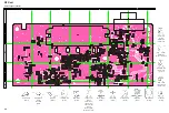
Incoming RF signals from the antenna connector are de-
livered to the RF Unit, and pass through a low-pass filter
(LPF) antenna switching network consisting of coils L1002,
L1003, capacitors C1004, C1009, C1016, C1019 and C1203
and antenna switching diodes
D1005
and
D1007
for de-
livery to the receiver front end.
Signals within the frequency range of the transceiver are
then passed through a varactor-tuned bandpass filter con-
sisting of L1008, and L1009 before RF amplification by
Q1011
(
).
The amplified RF is then band-pass filtered again by var-
actor-tuned resonators L1019, and L1023 to ensure pure
in-band input to 1st mixer
Q1026
(
).
Buffered output from the VCO Unit is amplified by
Q1021
(
) and low-pass filtered by L1030 / L1032 and
C1184 / C1188 / C1192, to provide a pure 1st local signal
between 178.25 and 218.25 MHz to the 1st mixer.
The 44.25MHz 1st mixer product then passes through dual
monolithic crystal filters XF1001, and is amplified by
Q1029
(
) and delivered to the input of the FM
IF subsystem IC
Q1028
(
).
This IC contains the 2nd mixer, 2nd local oscillator, limit-
er amplifier, FM detector, noise amplifier, and squelch
gates.
The 2nd LO in the IF-IC is produced from TCXO X1001
(14.600MHz) and the 1st IF is converted to 450kHz by the
2nd mixer and stripped of unwanted components by ce-
ramic filter CF1001 or CF1002. After passing through a
limiter amplifier, the signal is demodulated by the FM
detector
CD1001
(
).
Detected audio from Q1028 is applied to
Q2016
(
)
and audio low-pass filter. After volume adjustment by
Q2014
(
), the audio signal is amplified by the
AF power amplifier
Q1509
(
) and passed to
speaker jack.
4. Transmit Signal Path
Voice audio from the microphone is delivered via the
(Jack) Unit to the PANEL Unit, after passing through
amplifier
Q2022
(
), Mic gain-volume
Q2014
(
) pre-emphasis
Q2015
(
), and lim-
iter (IDC instantaneous deviation control), is adjusted for
optimum deviation level and delivered to the next stage.
Voice input from the microphone, CTCSS and DCS are
FM-modulated to the VCO and the reference frequency
oscillator of the synthesizer.
Synthesizer output, after passing through diode switch
D1022
(
), is amplified by driver
Q1022
(
) /
Q1025
(
) and power module
Q1014
(
) to obtain full RF output. The RF
energy then passes through antenna switch
D1005
/
D1007
and a low-pass filter circuit and finally to the antenna con-
nector.
RF output power from the final amplifier is sampled by
C M c o u p l e r a n d i s r e c t i f i e d b y
D 1 0 1 1
,
D 1 0 1 2
(
). The resulting DC is fed through Automatic
P o w e r C o n t r o l l e r
Q 1 0 0 3
(
) ,
Q 1 0 0 2
(
),
Q1032
(
), and TH1003 to trans-
mitter RF amplifier and thus the power output.
Generation of spurious products by the transmitter is min-
imized by the fundamental carrier frequency being equal
to the final transmitting frequency, modulated directly in
the transmit VCO. Additional harmonic suppression is
provided by a low-pass filter consisting of L1002, L1003,
L1005, L1011, C1004, C1009, C1016, C1019, C1025, C1034,
C1203 and C1283, resulting in more than 60dB of harmonic
suppression prior to delivery to the RF energy to the an-
tenna.
5. PLL Frequency Synthesizer
PLL frequency synthesizer consists of the VCO
Q1013
(
:RX) and
Q1015
(
:TX), VCO
buffers
Q1018
,
Q1020
,
Q1021
(all
), PLL sub-
system IC
Q1038
(
) and 14.6MHz reference
TCXO.
The frequency stability is ±2.5ppm within temperature
range of -20 to +55 degree. The output of the 14.6MHz
reference is applied to pin 1 of the PLL IC.
While receiving, VCO
Q1013
oscillates between 178.25 and
218.25 MHz according to the transceiver version and the
programmed receiving frequency. The VCO generates
178.25 to 218.25 MHz for providing to the first local sig-
nal. In TX, the VCO generates 134 to 174 MHz.
The output of the VCO is amplified by the Q1020 and rout-
Summary of Contents for VX-2500EV
Page 5: ...5 Block Diagram 1 ...
Page 6: ...6 Block Diagram 2 ...
Page 7: ...7 Interconnection Diagram ...
Page 8: ...8 Note ...
Page 18: ...18 RF Unit Jumper Information Note ...
Page 34: ...PANEL Unit 34 Note ...
Page 43: ...19 ...


