background image

4

Operating Manual Reprint 

(Partial)

K

EYPAD

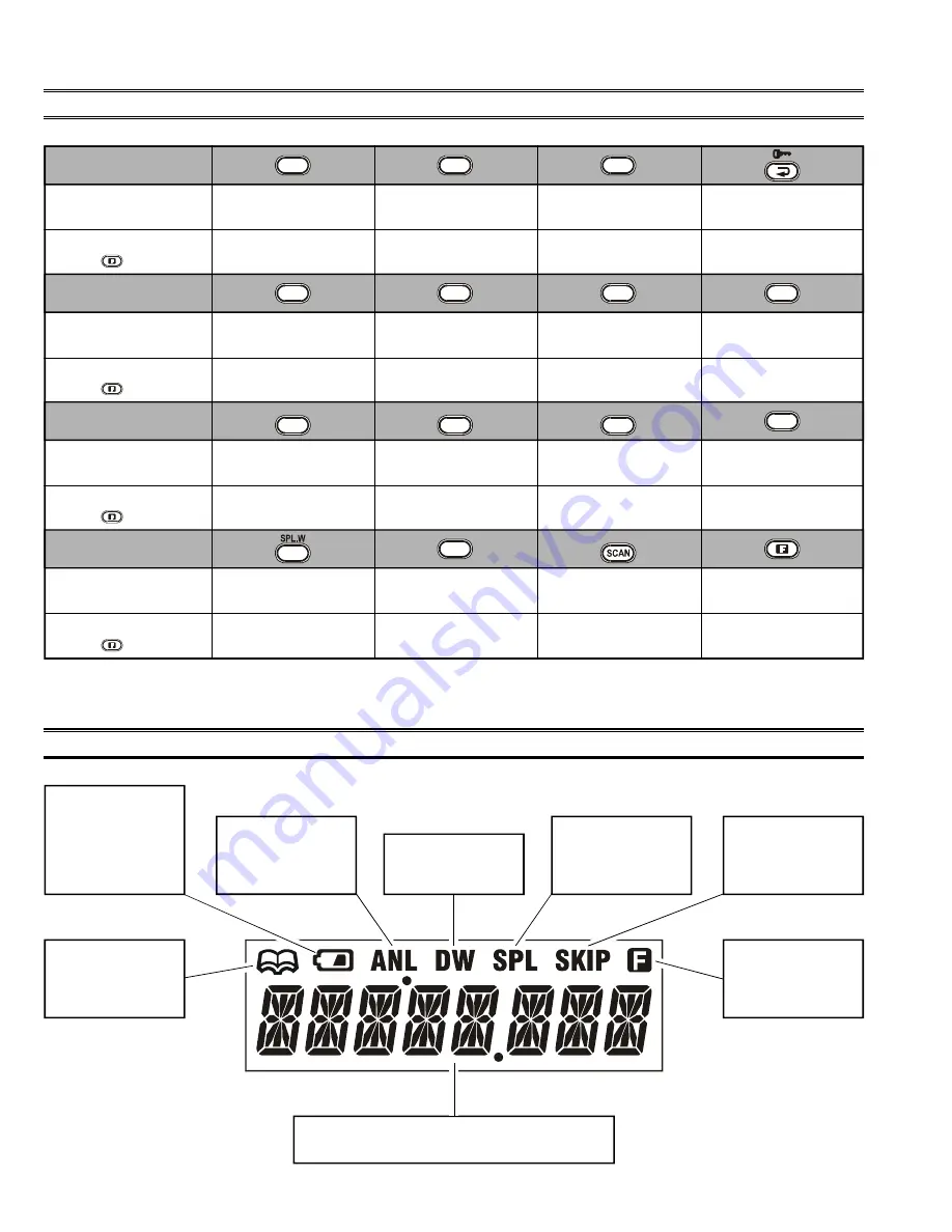
LCD D

ISPLAY

This indicator con-
firms that the A

UTO

-

MATIC

 N

OISE

 L

IMITER

 is

activated.

This icon is the “Low
Battery” indicator,
which blinks when
the battery voltage
becomes too low for
proper operation.

This indicator con-
f i r m s   t h a t   D

U A L

W

ATCH

 is active.

This indicator con-
firms that the “Split”
(Duplex) mode is
activated.

This indicator con-
firms that this chan-
nel will be skipped
during scan.

These digits provide frequency or alphanumeric
information about the channel you are using.

This icon indicates
t h a t   t h e   “ B o o k ”
Memory Bank is in
use.

This indicator con-
firms that 

Secondary

Key Function is ac-
tive.

Primary Function
(Press Key)

Secondary Function
(Press        +)

Primary Function
(Press Key)

Primary Function
(Press Key)

Primary Function
(Press Key)

Frequency Entry

Digit 1

Frequency Entry

Digit 2

Frequency Entry

Digit 3

Frequency Entry

Digit 4

Frequency Entry

Digit 5

Frequency Entry

Digit 6

Frequency Entry

Digit 7

Frequency Entry

Digit 8

Frequency Entry

Digit 9

Frequency Entry

Digit 0

Selects Memory Display

Type

Locks the Keypad

Selects Emergency

Channel (121.5 MHz)

None

None

None

None

None

None

Activates Automatic Noise

Limiter

Activates Split (Duplex)

mode

On/Off Switch

for Keypad Beeper

Allows Skipping of

Channel during Scan

Activates Scanning

Activates “Secondary”

Key mode

Activates Dual Watch

Memory “Write”

Command

Split-Memory “Write”

Command

Secondary Function
(Press        +)

Secondary Function
(Press        +)

Secondary Function
(Press        +)

None

None

None

None

3

2

1

4

5

6

121.5

ANL

SKIP

9

8

BEEP

7

SPL

MW

0

DW

Summary of Contents for VXA-150

Page 1: ...erted viewing when on your belt NOAA weather band monitoring 8 character Alpha Numeric Display 50 Memory Channels and 100 Book Memory Channels The following pages describe the Controls Connectors Accessories Options and Specification of the VXA 150 With proper care and operation the transceiver will provide many years of reliable communica tions VXA 150 VERTEX STANDARD CO LTD 4 8 8 Nakameguro Megu...

Page 2: ...r MR Memory Recall BOOK Pre Pro grammed Memories and WX Weather Channel Memories mode LCD Liquid Crystal Display The display shows the selected operating conditions as indicated on the next page The display may be changed to inverted viewing via the Menu BUSY TX Indicator Lamp This lamp glows green when a signal is being received and red when transmitting Loudspeaker The internal speaker is locate...

Page 3: ...nd hold this switch for 2 seconds to activate the back lighting lamp con tinuously To turn the lamp off press this switch again The LAMP switch may be configured in several ways via the Menu MIC EAR Jack You may connect the supplied CT 60 Headset Cable or the optional MH 44A4B Speaker Microphone to this jack Never connect any Speaker Microphone that is not recommended by the manufacturer Because t...

Page 4: ...ress Key Secondary Function Press Primary Function Press Key Primary Function Press Key Primary Function Press Key Frequency Entry Digit 1 Frequency Entry Digit 2 Frequency Entry Digit 3 Frequency Entry Digit 4 Frequency Entry Digit 5 Frequency Entry Digit 6 Frequency Entry Digit 7 Frequency Entry Digit 8 Frequency Entry Digit 9 Frequency Entry Digit 0 Selects Memory Display Type Locks the Keypad ...

Page 5: ...d first character appears press down on the CHANNEL selector knob momentarily to move on to the next char acter r Select succeeding characters in the same manner pressing down on the CHANNEL selector knob mo mentarily after each selection r After entering the entire name eight characters maxi mum press the MW SPL W key for 2 seconds to save all data for the channel r Turn the radio off then turn t...

Page 6: ... w FNB 64 Weight approx 0 75 lb 340 grams with FNB 64 antenna and belt clip Receiver Circuit Type Double conversion superheterodyne IFs 35 4 MHz 450 kHz Sensitivity 0 8 µV for 6 dB S N with 1 kHz 30 modulation Selectivity 8 kHz 6 dB Adjacent CH Selectivity 25 kHz 60 dB AF Output 7 2 V 0 4 W 8 Ohms 10 THD Transmitter Power Output 7 2 V 5 0 W PEP 1 5 W Carrier Power Frequency Stability Better than 1...

Page 7: ...on avoids damage to the electronics caused by voltage spikes Insert the distribution diskette into your 3 drive after booting DOS and make a copy of the diskette use the distribution diskette for archive purposes and use the disk copy for programming Place the CE32 copy diskette into your 3 drive usually Drive A and log onto this drive by typing A ENTER At this point you may make a directory for t...

Page 8: ...8 Notes ...

Page 9: ...11500 SPECIAL NUT RA0210900 WINDOW RA0211500 RUBBER CAP RA0111400 RING NUT RA0210600 RUBBER PACKING KNOB RA0248200 GROUND PLATE RA021020A RUBBER PACKING CASE CP7225001 REAR CASE ASS Y RA0210300 RUBBER KNOB PTT RA0385500 FRONT CASE ASS Y RA0384200 RUBBER KNOB AIR PRIN RA0123500 LATCH NAIL B CP7227001 BELT CLIP ASS Y SW UNIT MAIN UNIT RA0110200 HOLDER RUBBER M4090142B SPEAKER RA0128900 MYLAR SHEET R...

Page 10: ...10 Block Diagram ...

Page 11: ... mode detected audio from Q1049 is passed through the audio amplifier Q1028 1 NJM2904V and ANL circuit then applied to the AF amplifier Q1028 2 NJM2904V When ANL is on the ANL MUTE gate Q1027 UMG2 goes high the low pass filer limiter con sisting of capacitor C1124 resistors R1105 R1111 R1112 R1115 R1119 and diode D1023 BAS316 is activate thus reducing the pulse noises when impulse noise re ceived ...

Page 12: ...CO output is buffered by Q1029 and Q1036 and applied to the prescaler section of Q1032 There the VCO signal is divided by 64 or 65 ac cording to a control signal from the data latch section of Q1032 before being applied to the programmable divid er section of Q1032 The data latch section of Q1032 also receives serial dividing data from the microprocessor Q1014 M38254M6 which causes the pre divided...

Page 13: ...TT switch is closed pin 18 of Q1014 goes high This signals the microprocessor to activate the TX RX controller Q1017 UMG2N which cut off the receiver by disabling the 5 V supply bus at Q1020 DTA143EU which feeds the front end FM IF subsystem IC Q1049 and receiver VCO circuitry At the same time Q1037 UMW1 and Q1041 DTA143EU activates the transmit 5 V supply line to enable the transmitter ...

Page 14: ...sted the inter actions of some adjustments may require that more com plex adjustments be performed afterwards Do not attempt to perform only a single step unless it is clearly isolated electrically from all other steps Have all test equipment ready before beginning and follow all of the steps in a section in the order presented Correction of problems caused by misalignment result ing from use of i...

Page 15: ...lude Squelch Hysteresis Adjustment Squelch Threshold Adjustment Squelch Tight Adjustment To begin set the transceiver to 127 500 MHz and turn the transceiver off Then press and holding the LAMP switch PTT switch and the CHANNEL selector knob while turning the transceiver on Squelch Hysteresis Adjustment HSSQ r Press the CHANNEL selector knob then select the squelch hysteresis level using the CHANN...

Page 16: ...16 Note ...

Page 17: ...3 3 V 3 3 V 1 4 V 1 3 V 2 6 V 2 6 V 0 V 0 V 3 5 V 3 5 V 3 5 V 3 5 V 3 4 V 3 4 V SAVE ON 3 5 V SAVE OFF 0 V 0 V 1 8 V 1 8 V 1 6 V 1 6 V 7 0 V 7 0 V 7 3 V 7 3 V 0 V 3 7 V 0 V 1 7 V 0 V 1 7 V 0 V 1 7 V 0 V 1 7 V 0 V 1 7 V 3 4 V 0 V 3 3 V 0 V 0 V 0 V 0 V 0 V 0 V 0 V 0 V 0 6 V 0 V 0 V 0 4 V 0 6 V 0 9 V 0 V 0 9 V 0 9 V 1 7 V 1 7 V 3 5 V 3 5 V 0 V 3 4 V 0 V 0 V 1 5 V 0 V 1 5 V 0 V 1 0 V 1 0 V 6 4 V 6 0 V...

Page 18: ...MAIN Unit Note 18 ...

Page 19: ...26 R22 Q1051 1057 2SK2974 Q1052 DTC124TU 05 Q1019 DTA143EU 23 Q1018 2SA1602A MF Q1054 MC2850 A7 D1007 1018 1019 HSM88WA D1040 TK10931V Q1049 M38254M6 Q1014 Side A D C F E G 2 4 3 DTC143ZUA 123 Q1008 1031 RT1N241M N2 Q1026 1053 UMW1 W1 Q1055 S 80745SN Q1024 S 81235SGUP Q1030 ...

Page 20: ... K1 Q1047 UMW1 W1 Q1034 1037 1039 1046 DTA143EU 23 Q1020 1022 1041 RT1P441U P3 Q1025 UMZ2N Z2 Q1002 RT1N241M N2 Q1006 1021 1059 1060 MB15A01PFV Q1032 SB40W03T D1004 MC2850 A7 D1008 RN739F 5F D1015 1041 MC2848 A6 D1005 1031 AN6123MS Q1007 2SA1602A MF Q1035 AA1101F D1025 Side B 1 2 4 3 b a d c f e g 2SK880GR XG Q1042 NJM2902V Q1005 NJM2904V Q1028 02CZ2 0X 2 0X D1001 AK93C85AM Q1015 TDA7233D Q1009 ...

Page 21: ...10V BJ LMK105BJ104KV F K22108806 1 B g3 C 1033 AL ELECTRO CAP 220uF 10V SMG1AVB221M 220UF K40109027 1 A E3 C 1034 CHIP TA CAP 4 7uF 16V TEMSVA1C475M 8R K78120031 1 B e3 C 1036 CHIP CAP 0 01uF 16V B GRM36B103K16PT K22128804 1 B c2 C 1037 CHIP CAP 0 1uF 10V BJ LMK105BJ104KV F K22108806 1 B d4 C 1038 CHIP CAP 1uF 10V B GRM40B105K10PT K22100802 1 A G3 C 1040 CHIP CAP 0 001uF 50V B UMK105B102KW F K2217...

Page 22: ...1 A C3 C 1101 CHIP CAP 0 001uF 50V B UMK105B102KW F K22178829 1 B e2 C 1102 CHIP CAP 3pF 50V CJ UMK105CJ030CW F K22178251 1 B d2 C 1103 CHIP CAP 0 001uF 50V B UMK105B102KW F K22178829 1 B e2 C 1104 CHIP CAP 0 0022uF 50V B UMK105B222KW F K22178833 1 B e3 C 1105 CHIP CAP 0 01uF 16V B GRM36B103K16PT K22128804 1 B e3 C 1106 CHIP CAP 0 01uF 16V B GRM36B103K16PT K22128804 1 A C3 C 1107 CHIP CAP 0 01uF 1...

Page 23: ...P CAP 0 1uF 10V BJ LMK105BJ104KV F K22108806 1 A D2 C 1175 CHIP CAP 39pF 50V CH UMK105CH390JW F K22178272 1 B e1 C 1176 CHIP CAP 0 0047uF 25V B TMK105B472KW F K22148831 1 A D2 C 1177 CHIP CAP 0 001uF 50V B UMK105B102KW F K22178829 1 B c2 C 1178 CHIP CAP 0 1uF 10V BJ LMK105BJ104KV F K22108806 1 A D2 C 1180 CHIP TA CAP 0 22uF 20V TEMSVA21D224M 8R K78130022 1 A C2 C 1181 CHIP CAP 0 01uF 16V B GRM36B1...

Page 24: ...UMK105CK0R5CW F K22178247 1 A F1 C 1245 CHIP CAP 33pF 50V CH UMK105CH330JW F K22178270 1 B a1 C 1246 CHIP CAP 0 001uF 50V B UMK105B102KW F K22178829 1 B c1 C 1247 CHIP CAP 5pF 50V CH UMK105CH050CW F K22178253 1 B a1 C 1248 CHIP CAP 15pF 50V CH UMK105CH150JW F K22178262 1 B c1 C 1249 CHIP CAP 27pF 50V CH UMK105CH270JW F K22178268 1 B a1 C 1250 CHIP CAP 22pF 50V CH UMK105CH220JW F K22178266 1 B c1 C...

Page 25: ... B e1 L 1012 M RFC 0 022uH HK1608 22NJ T L1690520 1 B c1 L 1013 CHIP COIL 0 1uH LQN21AR10J04 L1690620 1 B d1 L 1014 M RFC 0 56uH LK1608 R56K T L1690415 1 A C2 L 1015 COIL E2 0 3 1 7 8T L L0022376 1 B b1 L 1016 COIL E2 0 28 1 0 6 5T R S L0022598 1 B b1 L 1017 CHIP COIL 0 1uH LQN21AR10J04 L1690620 1 B d1 L 1018 M RFC 0 56uH LK1608 R56K T L1690415 1 B e1 L 1019 M RFC 4 7uH LK1608 4R7K T L1690688 1 A ...

Page 26: ... Q 1050 TRANSISTOR 2SC4215Y TE85R G3342157Y 1 A C2 Q 1051 TRANSISTOR 2SC5226 5 TL G3352268E 1 A D1 Q 1052 FET 2SK2974 T11 G3829747 1 A E1 Q 1053 TRANSISTOR RT1N241M T11 1 G3070249 1 A D2 Q 1054 TRANSISTOR 2SA1602A T11 1F G3116028F 1 A D1 Q 1055 TRANSISTOR UMW1 TR G3070078 1 A D1 Q 1056 TRANSISTOR 2SC5226 5 TL G3352268E 1 B e1 Q 1057 TRANSISTOR 2SC5226 5 TL G3352268E 1 A D1 Q 1058 TRANSISTOR 2SC522...

Page 27: ...061 CHIP RES 6 8k 1 16W 5 RMC1 16S 682JTH J24189035 1 B d3 R 1062 CHIP RES 220k 1 16W 5 RMC1 16S 224JTH J24189053 1 B c3 R 1063 CHIP RES 56k 1 16W 5 RMC1 16S 563JTH J24189046 1 B g2 R 1064 CHIP RES 56k 1 16W 5 RMC1 16S 563JTH J24189046 1 B g2 R 1065 CHIP RES 39k 1 16W 5 RMC1 16S 393JTH J24189044 1 B g2 R 1066 CHIP RES 390k 1 16W 5 RMC1 16S 394JTH J24189056 1 B g2 R 1067 CHIP RES 47k 1 16W 5 RMC1 1...

Page 28: ...HIP RES 1k 1 16W 5 RMC1 16S 102JTH J24189025 1 B d1 R 1131 CHIP RES 47k 1 16W 5 RMC1 16S 473JTH J24189045 1 B f2 R 1132 CHIP RES 33k 1 16W 5 RMC1 16S 333JTH J24189043 1 B f1 R 1133 CHIP RES 47k 1 16W 5 RMC1 16S 473JTH J24189045 1 B d3 R 1134 CHIP RES 3 3k 1 16W 5 RMC1 16S 332JTH J24189031 1 B f1 R 1135 CHIP RES 100k 1 16W 5 RMC1 16S 104JTH J24189049 1 B f1 R 1136 CHIP RES 3 3k 1 16W 5 RMC1 16S 332...

Page 29: ...80 1 16W 5 RMC1 16S 181JTH J24189016 1 A F1 R 1200 CHIP RES 68k 1 16W 5 RMC1 16S 683JTH J24189047 1 A D1 R 1202 CHIP RES 560 1 16W 5 RMC1 16S 561JTH J24189022 1 B c1 R 1203 CHIP RES 560 1 16W 5 RMC1 16S 561JTH J24189022 1 B c1 R 1204 CHIP RES 33k 1 16W 5 RMC1 16S 333JTH J24189043 1 A F1 R 1206 CHIP RES 33k 1 16W 5 RMC1 16S 333JTH J24189043 1 A F1 R 1207 CHIP RES 47k 1 16W 5 RMC1 16S 473JTH J241890...

Page 30: ...YGC G2070810 1 B Q 2001 TRANSISTOR UMG2N TR G3070088 1 B R 2001 CHIP RES 330 1 16W 5 RMC1 16S 331JTH J24189019 1 B R 2002 CHIP RES 330 1 16W 5 RMC1 16S 331JTH J24189019 1 B S 2001 ROTARY ENCODER TP70N17AE20 Q9000738 1 B VR2001 POT TP76N00N 20KA SW J60800236 1 B VR Unit Parts List Side A Side B Circuit Diagram Parts Layout UMG2N G2 Q2001 12 22SURSYGC D2001 DESCRIPTION VALUE V W TOL VXSTD P N MFR S ...

Page 31: ...ALUE V W TOL VXSTD P N MFR S DESIG VERS LOT REF SIDE LAYADR PCB with Components CB1862001 Printed Circuit Board FR0026500 1 S 3001 TACT SWITCH SOP 114HST R66 5374 N5090107 1 A S 3002 TACT SWITCH SOP 114HST R66 5374 N5090107 1 A S 3003 TACT SWITCH SOP 114HST R66 5374 N5090107 1 A ...

Page 32: ...32 E C 0 3 6 N 9 0 0 Copyright 2001 VERTEX STANDARD CO LTD All rights reserved No portion of this manual may be reproduced without the permission of VERTEX STANDARD CO LTD Printed in Japan ...

Reviews: