26
Plasma TV Service Manual
05/01/2006
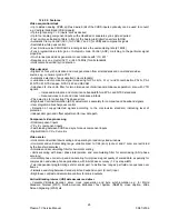
Audio clock generation
• Generation of a field-locked audio master clock to support a constant number of audio clocks per
video field
• Generation of an audio serial and left/right (channel)
Digital I/O interfaces
• Real-time signal port (R port), inclusive continuous line-locked reference clock and real-time status
information supporting RTC level 3.1 (refer to document “RTC Functional Specification” for details)
• Bidirectional expansion port (X-port) with half duplex functionality (D1), 8-bit Y-C
B
-C
R
– Output from decoder part, real-time and unscaled
– Input to scaler part, e.g. video from MPEG decoder (extension to 16-bit possible)
• Video image port (I-port) configurable for 8-bit data (extension to 16-bit possible) in master mode (own
clock), or slave mode (external clock), with auxiliary timing and handshake signals
• Discontinuous data streams supported
• 32-word ´ 4-byte FIFO register for video output data
• 28-word ´ 4-byte FIFO register for decoded VBI-data output
• Scaled 4 :2 :2, 4 :1 :1, 4 :2 :0, 4 :1 :0 Y-C
B
-C
R
output
• Scaled 8-bit luminance only and raw CVBS data output
• Sliced, decoded VBI-data output.
Miscellaneous
• Power-on control
• 5 V tolerant digital inputs and I/O ports
• Software controlled power saving standby modes supported
• Programming via serial I 2 C-bus, full read back ability by an external controller, bit rate up to 400
kbits/s
• Boundary scan test circuit complies with the “IEEE Std. 1149.b1 - 1994”
• BGA156 package.
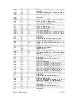
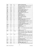
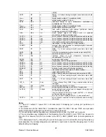
12.22.3. Pinning
SYMBOL PIN
TYPE
DESCRIPTION
XTOUT
A2
O
crystal oscillator output signal; auxiliary signal
XTALO
A3
O
24.576 MHz (32.11 MHz) crystal oscillator output; not
connected if TTL clock input of XTALI is used
V
SS(xtal)
A4
P
ground for crystal oscillator
TDO
A5
O
test data output for boundary scan test; note 2
XRDY
A6
O
task flag or ready signal from scaler, controlled by XRQT
XCLK
A7
I/O
clock I/O expansion port
XPD0
A8
I/O
LSB of expansion port data
XPD2
A9
I/O
MSB - 5 of expansion port data
XPD4
A10
I/O
MSB - 3 of expansion port data
XPD6
A11
I/O
MSB - 1 of expansion port data
TEST1
A12
I/pu
do not connect, reserved for future extensions and for testing:
scan input
TEST2
A13
I/pu
do not connect, reserved for future extensions and for testing:
scan input
AI41
B1
I
analog input 41
TEST3
B2
O
do not connect, reserved for future extensions and for testing
V
DD(xtal)
B3
P
supply voltage for crystal oscillator
XTALI
B4
I
input terminal for 24.576 MHz (32.11 MHz) crystal oscillator
or connection of external oscillator with TTL compatible
square wave clock signal
TDI
B5
I/pu
test data input for boundary scan test; note 2
TCK
B6
I/pu
test clock for boundary scan test; note 2
XDQ
B7
I/O
data qualifier for expansion port
XPD1
B8
I/O
MSB - 6 of expansion port data
XPD3
B9
I/O
MSB - 4 of expansion port data
XPD5
B10
I/O
MSB - 2 of expansion port data
XTRI
B11
I
X-port output control signal, affects all X-port pins (XPD7 to
XPD0, XRH, XRV, XDQ and XCLK), enable and active
polarity is under software control (bits XPE in subaddress
Summary of Contents for 17MB11
Page 1: ...50 PLASMA TV 17MB11 SERVICE MANUAL...
Page 50: ...47 Plasma TV Service Manual 25 08 2005 15 CIRCUIT DIAGRAMS...
Page 51: ...48 Plasma TV Service Manual 25 08 2005...
Page 52: ...49 Plasma TV Service Manual 25 08 2005...
Page 53: ...50 Plasma TV Service Manual 25 08 2005...
Page 54: ...51 Plasma TV Service Manual 25 08 2005...
Page 55: ...52 Plasma TV Service Manual 25 08 2005...
Page 56: ...53 Plasma TV Service Manual 25 08 2005...
Page 57: ...54 Plasma TV Service Manual 25 08 2005...

